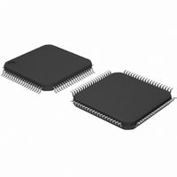
PCF8534AH/1,518 NXP Semiconductors, PCF8534AH/1,518 Datasheet - Page 6

PCF8534AH/1,518
Manufacturer Part Number
PCF8534AH/1,518
Description
IC LCD DVR UNVRSL LOW-MUX 80LQFP
Manufacturer
NXP Semiconductors
Datasheet
1.PCF8534AH1518.pdf
(44 pages)
Specifications of PCF8534AH/1,518
Package / Case
80-LQFP
Display Type
LCD
Configuration
60 Segment
Interface
I²C
Current - Supply
8µA
Voltage - Supply
1.8 V ~ 5.5 V
Operating Temperature
-40°C ~ 85°C
Mounting Type
Surface Mount
Number Of Digits
30
Number Of Segments
240
Maximum Clock Frequency
400 KHz
Operating Supply Voltage
1.8 V to 5.5 V
Maximum Power Dissipation
400 mW
Maximum Operating Temperature
+ 85 C
Maximum Supply Current
50 mA
Minimum Operating Temperature
- 40 C
Lead Free Status / RoHS Status
Lead free / RoHS Compliant
Digits Or Characters
-
Lead Free Status / Rohs Status
Details
Other names
935284829518
PCF8534AH/1-T
PCF8534AH/1-T
PCF8534AH/1-T
PCF8534AH/1-T
Available stocks
Company
Part Number
Manufacturer
Quantity
Price
Company:
Part Number:
PCF8534AH/1,518
Manufacturer:
NXP Semiconductors
Quantity:
10 000
Part Number:
PCF8534AH/1,518
Manufacturer:
NXP/恩智浦
Quantity:
20 000
NXP Semiconductors
PCF8534A_3
Product data sheet
7.1 Power-on reset
7.2 LCD bias generator
7.3 LCD voltage selector
The host microprocessor or microcontroller maintains the 2-line I
channel with the PCF8534A.
Biasing voltages for the multiplexed LCD waveforms are generated internally, removing
the need for an external bias generator. The internal oscillator is selected by connecting
pin OSC to V
power supplies (pins V
At power-on the PCF8534A resets to a default starting condition:
Do not transfer data on the I
complete.
Fractional LCD biasing voltages are obtained from an internal voltage divider comprising
three series resistors connected between pins V
switched out of the circuit to provide the
configuration.
The LCD voltage selector coordinates the multiplexing of the LCD based on the selected
LCD drive configuration. The operation of the voltage selector is controlled by mode set
commands from the command decoder.
Fig 4.
•
•
•
•
•
•
•
•
All backplane outputs are set to V
All segment outputs are set to V
The selected drive mode is: 1:4 multiplex with
Blinking is switched off
Input and output bank selectors are reset
The I
The data pointer and the subaddress counter are cleared (set to logic 0)
The display is disabled
V
V
DD
SS
2
Typical system configuration
C-bus interface is initialized
CONTROLLER
PROCESSOR/
MICRO-
MICRO-
SS
HOST
. The only other connections required to complete the system are the
R
2C
Rev. 03 — 10 November 2008
t
r
b
DD
, V
SS
2
C-bus after a power-on for 1 ms to enable the reset action to
and V
OSC
SDA
SCL
LCD
LCD
LCD
A0
) and the LCD panel selected for the application.
1
2
PCF8534A
Universal LCD driver for low multiplex rates
bias voltage level for the 1:2 multiplex
A1
V
DD
A2
LCD
V
1
LCD
SA0
3
and V
bias
V
SS
60 segment drives
SS
4 backplanes
. The center resistor is
2
C-bus communication
PCF8534A
© NXP B.V. 2008. All rights reserved.
LCD PANEL
(up to 240
elements)
001aah616
6 of 44


