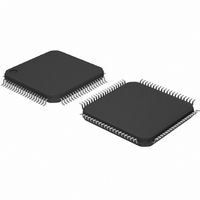
PCF8534AH/1,518 NXP Semiconductors, PCF8534AH/1,518 Datasheet - Page 17

PCF8534AH/1,518
Manufacturer Part Number
PCF8534AH/1,518
Description
IC LCD DVR UNVRSL LOW-MUX 80LQFP
Manufacturer
NXP Semiconductors
Datasheet
1.PCF8534AH1518.pdf
(44 pages)
Specifications of PCF8534AH/1,518
Package / Case
80-LQFP
Display Type
LCD
Configuration
60 Segment
Interface
I²C
Current - Supply
8µA
Voltage - Supply
1.8 V ~ 5.5 V
Operating Temperature
-40°C ~ 85°C
Mounting Type
Surface Mount
Number Of Digits
30
Number Of Segments
240
Maximum Clock Frequency
400 KHz
Operating Supply Voltage
1.8 V to 5.5 V
Maximum Power Dissipation
400 mW
Maximum Operating Temperature
+ 85 C
Maximum Supply Current
50 mA
Minimum Operating Temperature
- 40 C
Lead Free Status / RoHS Status
Lead free / RoHS Compliant
Digits Or Characters
-
Lead Free Status / Rohs Status
Details
Other names
935284829518
PCF8534AH/1-T
PCF8534AH/1-T
PCF8534AH/1-T
PCF8534AH/1-T
Available stocks
Company
Part Number
Manufacturer
Quantity
Price
Company:
Part Number:
PCF8534AH/1,518
Manufacturer:
NXP Semiconductors
Quantity:
10 000
Part Number:
PCF8534AH/1,518
Manufacturer:
NXP/恩智浦
Quantity:
20 000
NXP Semiconductors
PCF8534A_3
Product data sheet
7.12 Subaddress counter
7.13 Output bank selector
7.14 Input bank selector
The storage of display data is conditioned by the contents of the subaddress counter.
Storage is allowed only when the contents of the subaddress counter agree with the
hardware subaddress applied to A0, A1 and A2. The subaddress counter value is defined
by the device select command (see
and the hardware subaddress do not agree then data storage is blocked but the data
pointer will be incremented as if data storage had taken place.
In cascaded applications each PCF8534A in the cascade must be addressed separately.
Initially, the first PCF8534A is selected by sending the device select command matching
the first device's hardware subaddress. Then the data pointer is set to the preferred
display RAM address by sending the load data pointer command.
Once the display RAM of the first PCF8534A has been written, the second PCF8534A is
selected by sending the device select command again. This time however the command
matches the second device's hardware subaddress. Next the load data pointer command
is sent to select the preferred display RAM address of the second PCF8534A.
This last step is very important because during writing data to the first PCF8534A, the
data pointer of the second PCF8534A is incremented. In addition, the hardware
subaddress should not be changed whilst the device is being accessed on the I
interface.
The output bank selector (see
address for transfer to the display register. The actual bit selected depends on the LCD
drive mode in operation and on the instant in the multiplex sequence.
The SYNC signal resets these sequences to the following starting points: bit 3 for
1:4 multiplex, bit 2 for 1:3 multiplex, bit 1 for 1:2 multiplex and bit 0 for static mode.
The PCF8534A includes a RAM bank switching feature in the static and 1:2 multiplex
drive modes. In static drive mode, the bank select command may request the contents of
bit 2 to be selected for display instead of the contents of bit 0. In 1:2 multiplex drive mode,
the contents of bits 2 and 3 may be selected instead of bits 0 and 1. This enables
preparation of display information in an alternative bank and the ability to switch to it once
it has been assembled.
The input bank selector loads display data into the display RAM based on the selected
LCD drive configuration. Using the bank select command, display data can be loaded in
bit 2 into static drive mode or in bits 2 and 3 into 1:2 multiplex drive mode. The input bank
selector functions independently to the output bank selector.
•
•
•
•
In 1:4 multiplex mode: all RAM addresses of bit 0 are selected, followed sequentially
by the contents of bit 1, bit 2 and then bit 3.
In 1:3 multiplex mode: bits 0, 1 and 2 are selected sequentially.
In 1:2 multiplex mode: bits 0 and 1 are selected.
In the static mode: bit 0 is selected.
Rev. 03 — 10 November 2008
Table
Table
13), selects one of the four bits per display RAM
12). If the contents of the subaddress counter
Universal LCD driver for low multiplex rates
PCF8534A
© NXP B.V. 2008. All rights reserved.
2
C-bus
17 of 44


