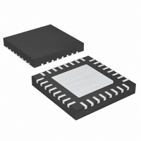
MAX5072ETJ+ Maxim Integrated Products, MAX5072ETJ+ Datasheet - Page 10

MAX5072ETJ+
Manufacturer Part Number
MAX5072ETJ+
Description
IC CONV BUCK/BOOST 32-TQFN
Manufacturer
Maxim Integrated Products
Type
Step-Down (Buck), Step-Up (Boost)r
Datasheet
1.MAX5072ETJ.pdf
(27 pages)
Specifications of MAX5072ETJ+
Internal Switch(s)
Yes
Synchronous Rectifier
No
Number Of Outputs
2
Voltage - Output
0.8 ~ 28 V
Current - Output
1A, 2A
Frequency - Switching
200kHz ~ 2.2MHz
Voltage - Input
4.5 ~ 23 V
Operating Temperature
-40°C ~ 85°C
Mounting Type
Surface Mount
Package / Case
32-TQFN Exposed Pad
Power - Output
2.76W
Output Voltage
5.2 V
Output Current
2 A
Input Voltage
5.5 V to 23 V
Supply Current
2.2 mA
Switching Frequency
1250 KHz
Mounting Style
SMD/SMT
Maximum Operating Temperature
+ 85 C
Minimum Operating Temperature
- 40 C
Lead Free Status / RoHS Status
Lead free / RoHS Compliant
2.2MHz, Dual-Output Buck or Boost
Converter with POR and Power-Fail Output
10
13, 14
21, 22
26, 27
PIN
11
12
15
16
17
18
19
20
23
24
25
______________________________________________________________________________________
BST1/VDD1
SOURCE1
PGOOD1
BYPASS
DRAIN1
COMP1
NAME
FSEL1
OSC
RST
FB1
EN1
MR
V+
VL
Oscillator Frequency Set Input. Connect a resistor from OSC to SGND (R
frequency (see the Oscillator section). Set R
input frequency when using external synchronization (0.2f
when an external clock is connected to the SYNC input.
Input Supply Voltage. V+ voltage range from 5.5V to 23V. Connect the V+ and VL together for 4.5V to
5.5V input operation. Bypass with a minimum 0.1µF ceramic capacitor to SGND.
Internal 5.2V Linear Regulator Output. Use VL to drive the high-side switch at BST1/VDD1 and
BST2/VDD2. Bypass VL with a 0.1µF capacitor to PGND and a 4.7µF ceramic capacitor to SGND.
2.0V Output. Bypass to SGND with a 0.22µF or greater ceramic capacitor.
Active-Low Manual Reset Input. Drive MR low to initiate a reset. RST remains asserted while MR is low
and for 180ms (t
pulled high by a 44kΩ resistor and can be left open if not used.
Open-Drain Reset Output. RST remains low when either output voltage is below 92.5% of its regulation
point or while MR is low. After soft-start is completed and both outputs exceed 92.5% of their nominal
output voltage, RST becomes high impedance after a 180ms (typ) delay. RST remains high impedance
as long as both outputs maintain regulation.
Compensation Connection for Converter 1 (See the Compensation Section)
Feed b ack Inp ut for C onver ter 1. C onnect FB1 to a r esi sti ve d i vi d er b etw een conver ter 1’ s outp ut and S GN D
to p r og r am the outp ut vol tag e. To set the outp ut vol tag e b el ow 0.8V , connect FB1 to a r esi sti ve vol tag e-
d i vi d er fr om BY P AS S to r eg ul ator 1’ s outp ut ( Fi g ur e 6) . S ee the S etti ng the O utp ut V ol tag e secti on.
Acti ve- H i g h E nab l e Inp ut for C onver ter 1. D r i ve E N 1 l ow to shut d ow n conver ter 1, d r i ve E N 1 hi g h for nor m al
op er ati on. U se E N 1 i n conj uncti on w i th E N 2 for sup p l y seq uenci ng . C onnect to V L for al w ays- on op er ati on.
Connection to the Converter 1 Internal MOSFET Drain.
Buck conver ter op er ati on— use the M OS FE T as a hi g h- si d e sw i tch and connect D RAIN 1 to the i np ut sup p l y.
Boost converter operation—use the MOSFET as a low-side switch and connect DRAIN1 to the inductor
and diode junction.
Buck Converter Operation—Bootstrap Flying-Capacitor Connection for Converter 1. Connect BST1/VDD1
to an external ceramic capacitor and diode according to the Standard Application Circuit (Figure 1).
Boost Converter Operation—Driver Bypass Capacitor Connection. Connect a low-ESR 0.1µF ceramic
capacitor from BST1/VDD1 to PGND (Figure 9).
Converter 1 Frequency Select Input. Connect FSEL1 to VL for normal operation. Connect FSEL1 to SGND
to reduce converter 1’s switching frequency to 1/2 converter 2’s switching frequency (converter 1
switching frequency will be 1/4 the SYNC frequency). Do not leave FSEL1 unconnected.
Converter 1 Power-Good Output. Open-drain output goes low when converter 1’s output falls below
92.5% of its set regulation voltage. Use PGOOD1 and EN2 to sequence the converters.
Connection to the Converter 1 Internal MOSFET Source.
Buck Converter Operation—connect SOURCE1 to the switched side of the inductor as shown in Figure 1.
Boost Converter Operation—connect SOURCE1 to PGND.
RP
) after MR returns high. MR requires no external debounce circuitry. MR is internally
OSC
FUNCTION
for equal to or lower oscillator frequency than the SYNC
Pin Description (continued)
SYNC
< f
OSC
< 1.2f
OSC
) to set the switching
SYNC
). R
OSC
is still required


