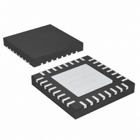
MAX5072ETJ+ Maxim Integrated Products, MAX5072ETJ+ Datasheet - Page 16

MAX5072ETJ+
Manufacturer Part Number
MAX5072ETJ+
Description
IC CONV BUCK/BOOST 32-TQFN
Manufacturer
Maxim Integrated Products
Type
Step-Down (Buck), Step-Up (Boost)r
Datasheet
1.MAX5072ETJ.pdf
(27 pages)
Specifications of MAX5072ETJ+
Internal Switch(s)
Yes
Synchronous Rectifier
No
Number Of Outputs
2
Voltage - Output
0.8 ~ 28 V
Current - Output
1A, 2A
Frequency - Switching
200kHz ~ 2.2MHz
Voltage - Input
4.5 ~ 23 V
Operating Temperature
-40°C ~ 85°C
Mounting Type
Surface Mount
Package / Case
32-TQFN Exposed Pad
Power - Output
2.76W
Output Voltage
5.2 V
Output Current
2 A
Input Voltage
5.5 V to 23 V
Supply Current
2.2 mA
Switching Frequency
1250 KHz
Mounting Style
SMD/SMT
Maximum Operating Temperature
+ 85 C
Minimum Operating Temperature
- 40 C
Lead Free Status / RoHS Status
Lead free / RoHS Compliant
2.2MHz, Dual-Output Buck or Boost
Converter with POR and Power-Fail Output
Figure 4. Power-Supply Sequencing Configurations
The MAX5072 contains an uncommitted comparator
with an open-drain output. The inverting input of the
comparator is connected to an internal precision 0.78V
reference. Connect the noninverting input (PFI) to V
through a resistor-divider to program the input trip
threshold (V
low when PFI drops below 0.78V. PFI provides 20mV
hysteresis to avoid glitches during transition. The PFO
signal provides an advance signal to the processor
before the converter 1/converter 2 loses regulation. The
input trip threshold (V
advance signaling before the outputs drop to 92.5% of
the regulation voltage.
The input capacitors hold charge and provide energy
to the converter after V
time (t
age drops below V
lation at the low end of the input voltage range V
(Figure 5). Use the following equations to calculate the
resistor-divider and the C
hold-up time.
where η1 and η2 are efficiencies of the converter 1 and
converter 2, respectively.
16
SEQUENCING—OUTPUT 2 DELAYED WITH RESPECT TO OUTPUT 1.
OUTPUT2
______________________________________________________________________________________
HOLD
VL
C
IN
) is defined as the time when the input volt-
Dying Gasp Comparator (PFI/PFO)
TRIP
=
⎛
⎝
2
). The power-fail output (PFO) is pulled
V
⎛
⎜
⎝
TRIP
2
P
VL
TRIP
OUT1
η
1
TRIP
DRAIN2
SOURCE2
−
FB2
EN2
IN
and the output falls out of regu-
V
+
2
is disconnected. The hold-up
) can be adjusted to provide
VL
MAX5072
P
IN(MIN)
IN
OUT2
η
2
required for the proper
SOURCE1
V+
PGOOD1
DRAIN1
⎞
⎟
⎠
⎞
⎠
FB1
EN1
×
t
HOLD
VL
IN(MIN)
OUTPUT1
IN
V
IN
R1/C1 AND R2/C2 ARE SIZED FOR REQUIRED SEQUENCING.
OUTPUT2
R
The internal switch current of each converter is sensed
using an internal current mirror. Converter 1 and con-
verter 2 have 2A and 1A internal switches. When the
peak switch current crosses the current-limit threshold
of 3A (typ) and 1.8A (typ) for converter 1 and converter
2, respectively, the on cycle is terminated immediately
and the inductor is allowed to discharge. The next
cycle resumes at the next clock pulse.
Figure 5. Dying Gasp Feature Monitors Input Supply
2
OUTPUT2
can be any value from 10kΩ to 100kΩ (Figure 5).
VL
R2
C2
VL
VL
R1 R2
DRAIN2
SOURCE2
FB2
EN2
DRAIN2
SOURCE2
=
VL
VL
MAX5072
MAX5072
⎛
⎜
⎝
V
0.78
SOURCE1
SOURCE1
TRIP
V+
V+
DRAIN1
DRAIN1
EN1
PFO
FB1
PFI
−
1
⎞
⎟
⎠
VL
C1
Current Limit
R1
PFO
CIN
OUTPUT1
VL
OUTPUT1
V
V
IN
R1
R2
IN


