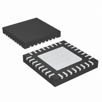
MAX5072ETJ+ Maxim Integrated Products, MAX5072ETJ+ Datasheet - Page 17

MAX5072ETJ+
Manufacturer Part Number
MAX5072ETJ+
Description
IC CONV BUCK/BOOST 32-TQFN
Manufacturer
Maxim Integrated Products
Type
Step-Down (Buck), Step-Up (Boost)r
Datasheet
1.MAX5072ETJ.pdf
(27 pages)
Specifications of MAX5072ETJ+
Internal Switch(s)
Yes
Synchronous Rectifier
No
Number Of Outputs
2
Voltage - Output
0.8 ~ 28 V
Current - Output
1A, 2A
Frequency - Switching
200kHz ~ 2.2MHz
Voltage - Input
4.5 ~ 23 V
Operating Temperature
-40°C ~ 85°C
Mounting Type
Surface Mount
Package / Case
32-TQFN Exposed Pad
Power - Output
2.76W
Output Voltage
5.2 V
Output Current
2 A
Input Voltage
5.5 V to 23 V
Supply Current
2.2 mA
Switching Frequency
1250 KHz
Mounting Style
SMD/SMT
Maximum Operating Temperature
+ 85 C
Minimum Operating Temperature
- 40 C
Lead Free Status / RoHS Status
Lead free / RoHS Compliant
In deep overload or short-circuit conditions when the
FB voltage drops below 0.4V, the switching frequency
is reduced to 1/4 x f
inductor to discharge. During overload conditions, if the
voltage across the inductor is not high enough to allow
for the inductor current to properly discharge, current
runaway may occur. Current runaway can destroy the
device in spite of internal thermal-overload protection.
Reducing the switching frequency during overload con-
ditions prevents current runaway.
During continuous short circuit or overload at the out-
put, the power dissipation in the IC can exceed its limit.
Internal thermal shutdown is provided to avoid irre-
versible damage to the device. When the die tempera-
ture or junction temperature exceeds +150°C, an
on-chip thermal sensor shuts down the device, forcing
the internal switches to turn off, allowing the IC to cool.
The thermal sensor turns the part on again after the
junction temperature cools by +30°C. During thermal
shutdown, both regulators shut down, RST goes low,
and soft-start resets.
The controller generates the clock signal by dividing
down the internal oscillator or the SYNC input signal
when driven by an external oscillator. The switching
frequency equals half the oscillator frequency (f
f
resistor (R
relationship between f
where f
For example, a 1250kHz switching frequency is set with
R
lower inductor values and less output capacitance.
Consequently, peak currents and I
at higher switching frequencies, but core losses, gate-
charge currents, and switching losses increase.
A rising clock edge on SYNC is interpreted as a syn-
chronization input. If the SYNC signal is lost, the inter-
nal oscillator takes control of the switching rate,
returning the switching frequency to that set by R
This maintains output regulation even with intermittent
SYNC signals. When an external synchronization signal
is used, R
to be lower than or equal to the SYNC rate (f
OSC
OSC
/ 2). The internal oscillator frequency is set by a
= 10kΩ. Higher frequencies allow designs with
SW
OSC
OSC
and f
Converter with POR and Power-Fail Output
Setting the Switching Frequency
should be set for the oscillator frequency
) connected from OSC to SGND. The
Applications Information
OSC
R
Thermal-Overload Protection
OSC
______________________________________________________________________________________
SW
are in hertz, and R
SW
=
to provide sufficient time for the
12.5
and R
f
SW
2.2MHz, Dual-Output Buck or Boost
×
OSC
10
2
9
is:
R losses are lower
OSC
SYNC
is in ohms.
).
SW
OSC
=
.
Although the MAX5072 converters can operate from
input supplies ranging from 4.5V to 23V, the input volt-
age range can be effectively limited by the MAX5072
duty-cycle limitations for a given output voltage. The
maximum input voltage is limited by the minimum on-
time (t
where t
limited by the maximum duty cycle (D
where V
inductor discharge path, which includes the forward
voltage drop (V
the inductor, and the PC board resistance. V
the total resistance in the charging path, which includes
the on-resistance of the high-side switch, the series
resistance of the inductor, and the PC board resistance.
For 0.8V or greater output voltages, connect a voltage-
divider from OUT_ to FB_ to SGND (Figure 6). Select
R
Calculate R
equation:
where V
and V
Figure 6. Adjustable Output Voltage
B
MAX5072
(FB_ to SGND resistor) to between 1kΩ and 10kΩ.
V
IN MIN
OUT_
ON(MIN)
(
ON(MIN)
FB_
DROP1
LX_
FB_
V
OUT_
)
can range from V
= 0.8V (see the Electrical Characteristics table)
A
=
V
> 0.8V
):
(OUT_ to FB_ resistor) with the following
⎡
⎢
⎣
IN MAX
D
V
is the total parasitic voltage drops in the
is 100ns. The minimum input voltage is
(
OUT
R
) of the rectifier, the series resistance of
A
=
0 88
)
+
.
R
≤
V
R
R
B
A
B
Effective Input Voltage Range
DROP
t
ON MIN
⎡
⎢
⎢
⎣
⎛
⎜
⎝
FB_
Setting the Output Voltage
V
(
V
OUT
MAX5072
1
FB
V
⎤
⎥ +
⎦
to 28V (boost operation).
OUT
)
BYPASS
⎞
⎟
⎠
V
×
FB_
LX_
−
DROP
Buck Converter
V
1
OUT_
f
SW
⎤
⎥
⎥
⎦
MAX
< 0.8V
2
= 0.88):
−
V
DROP
DROP2
R
R
C
A
1
17
is


