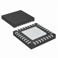
MAX5072ETJ+ Maxim Integrated Products, MAX5072ETJ+ Datasheet - Page 12

MAX5072ETJ+
Manufacturer Part Number
MAX5072ETJ+
Description
IC CONV BUCK/BOOST 32-TQFN
Manufacturer
Maxim Integrated Products
Type
Step-Down (Buck), Step-Up (Boost)r
Datasheet
1.MAX5072ETJ.pdf
(27 pages)
Specifications of MAX5072ETJ+
Internal Switch(s)
Yes
Synchronous Rectifier
No
Number Of Outputs
2
Voltage - Output
0.8 ~ 28 V
Current - Output
1A, 2A
Frequency - Switching
200kHz ~ 2.2MHz
Voltage - Input
4.5 ~ 23 V
Operating Temperature
-40°C ~ 85°C
Mounting Type
Surface Mount
Package / Case
32-TQFN Exposed Pad
Power - Output
2.76W
Output Voltage
5.2 V
Output Current
2 A
Input Voltage
5.5 V to 23 V
Supply Current
2.2 mA
Switching Frequency
1250 KHz
Mounting Style
SMD/SMT
Maximum Operating Temperature
+ 85 C
Minimum Operating Temperature
- 40 C
Lead Free Status / RoHS Status
Lead free / RoHS Compliant
2.2MHz, Dual-Output Buck or Boost
Converter with POR and Power-Fail Output
The MAX5072 converter uses a pulse-width modulation
(PWM) voltage-mode control scheme for each out-of-
phase controller. It is nonsynchronous rectification and
uses an external low-forward-drop Schottky diode for
rectification. The controller generates the clock signal
by dividing down the internal oscillator or the SYNC
input when driven by an external clock, so each con-
troller’s switching frequency equals half the oscillator
frequency (f
tance error amplifier produces an integrated error volt-
age at the COMP pin, providing high DC accuracy. The
voltage at COMP sets the duty cycle using a PWM
comparator and a ramp generator. At each rising edge
of the clock, converter 1’s high-side n-channel MOSFET
turns on and remains on until either the appropriate or
maximum duty cycle is reached, or the maximum cur-
rent limit for the switch is detected. Converter 2 oper-
ates out-of-phase, so the second high-side MOSFET
turns on at each falling edge of the clock.
In the case of buck operation (Figure 1), during each
high-side MOSFET’s on-time, the associated inductor
current ramps up. During the second half of the switch-
ing cycle, the high-side MOSFET turns off and forward
biases the Schottky rectifier. During this time, the
SOURCE voltage is clamped to 0.4V (V
ground. The inductor releases the stored energy as its
current ramps down, and provides current to the out-
put. The bootstrap capacitor is also recharged from the
inductance energy when the MOSFET turns off. The cir-
cuit goes in discontinuous conduction mode operation
at light load, when the inductor current completely dis-
charges before the next cycle commences. Under
overload conditions, when the inductor current exceeds
the peak current limit of the respective switch, the high-
side MOSFET turns off quickly and waits until the next
clock cycle.
In the case of boost operation, the MOSFET is a low-
side switch (Figure 9). During each on-time, the induc-
tor current ramps up. During the second half of the
switching cycle, the low-side switch turns off and for-
ward biases the Schottky diode. During this time the
DRAIN voltage is clamped to 0.4V (V
and the inductor provides energy to the output as well
as replenishes the output capacitor charge.
The internal oscillator generates the 180° out-of-phase
clock signal required by each regulator. The internal
oscillator frequency is programmable from 400kHz to
4.4MHz using a single 1% resistor at R
lowing equation to calculate R
12
Internal Oscillator/Out-of-Phase Operation
______________________________________________________________________________________
SW
= f
OSC
Detailed Description
/ 2). An internal transconduc-
OSC
:
PWM Controller
OSC
D
) above V
. Use the fol-
D
) below
OUT_
where f
and R
The two independent regulators in the MAX5072 switch
180° out-of-phase to reduce input filtering require-
ments, to reduce electromagnetic interference (EMI),
and to improve efficiency. This effectively lowers com-
ponent cost and saves board space, making the
MAX5072 ideal for cost-sensitive applications.
With dual synchronized out-of-phase operation, the
MAX5072’s high-side MOSFETs turn on 180° out-of-
phase. The instantaneous input current peaks of both
regulators do not overlap, resulting in reduced RMS rip-
ple current and input voltage ripple. This reduces the
required input capacitor ripple current rating, allows for
fewer or less expensive capacitors, and reduces
shielding requirements for EMI. The out-of-phase wave-
forms in the Typical Operating Characteristics demon-
strate synchronized 180° out-of-phase operation.
The main oscillator can be synchronized to the system
clock by applying an external clock (f
The f
ating frequency of an individual converter. Use a TTL
logic signal for the external clock with at least a 100ns
pulse width. R
synchronization. Program the internal oscillator fre-
quency so 0.2f
edge of f
MOSFET (see Figure 3).
where f
and R
Two MAX5072s can be connected in master-slave con-
figuration for four ripple-phase operation. The MAX5072
provides a clock output (CLKOUT) that is 45° phase-
shifted with respect to the internal switch turn-on edge.
Feed the CLKOUT of the master to the SYNC input of
the slave. The effective input ripple switching frequency
shall be four times the individual converter’s switching
frequency. When driving the master converter using
external clock at SYNC, set the clock duty cycle to 50%
for a 90° phase-shifted operation.
SYNC
OSC
OSC
OSC
OSC
SYNC
in ohms.
in ohms, f
frequency must be twice the required oper-
is the internal oscillator frequency in hertz
is the internal oscillator frequency in hertz
OSC
synchronizes the turn-on edge of internal
SYNC
Synchronization (SYNC)/Clock
R
OSC
R
is still required when using external
OSC
OSC
< f
=
= 2 x f
=
25
OSC
25
f
OSC
×
f
OSC
×
< 1.2f
SW
10
Output (CLKOUT)
10
9
.
9
SYNC
SYNC
. The rising
) at SYNC.


