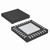
MAX5072ETJ+ Maxim Integrated Products, MAX5072ETJ+ Datasheet - Page 11

MAX5072ETJ+
Manufacturer Part Number
MAX5072ETJ+
Description
IC CONV BUCK/BOOST 32-TQFN
Manufacturer
Maxim Integrated Products
Type
Step-Down (Buck), Step-Up (Boost)r
Datasheet
1.MAX5072ETJ.pdf
(27 pages)
Specifications of MAX5072ETJ+
Internal Switch(s)
Yes
Synchronous Rectifier
No
Number Of Outputs
2
Voltage - Output
0.8 ~ 28 V
Current - Output
1A, 2A
Frequency - Switching
200kHz ~ 2.2MHz
Voltage - Input
4.5 ~ 23 V
Operating Temperature
-40°C ~ 85°C
Mounting Type
Surface Mount
Package / Case
32-TQFN Exposed Pad
Power - Output
2.76W
Output Voltage
5.2 V
Output Current
2 A
Input Voltage
5.5 V to 23 V
Supply Current
2.2 mA
Switching Frequency
1250 KHz
Mounting Style
SMD/SMT
Maximum Operating Temperature
+ 85 C
Minimum Operating Temperature
- 40 C
Lead Free Status / RoHS Status
Lead free / RoHS Compliant
Figure 1. MAX5072 Dual Buck Regulator Application Circuit
28, 30
31, 32
OUTPUT
2.5V/1A
PIN
EP
29
V
IN
SGND
= 5.5V TO 23V
Converter with POR and Power-Fail Output
SOURCE2
NAME
PGND
SGND
SGND
______________________________________________________________________________________
PGND
VL
PFO
VL
Power Ground. Connect rectifier diode anode, input capacitor negative, output capacitor negative, and
VL bypass capacitor returns to PGND.
S i g nal G r ound . C onnect S G N D to the exp osed p ad . C onnect S G N D and P G N D tog ether at a si ng l e p oi nt.
Connection to the Converter 2 Internal MOSFET Source.
Buck Converter Operation—connect SOURCE2 to the switched side of the inductor as shown in Figure 1.
Boost Converter Operation—connect SOURCE2 to PGND (Figure 9).
Exposed Paddle. Connect to SGND. Solder EP to the SGND plane for better thermal performance.
DYING GASP
OFF
CLOCK
2.2MHz, Dual-Output Buck or Boost
OUT
ON
1
2
3
4
5
6
7
8 PFO
CLKOUT
BST2/VDD2
DRAIN2
DRAIN2
EN2
FB2
COMP2
SYSTEM
CLOCK
32
9
31
10
EP
11
30
SGND*
MAX5072
12
29
13
28
PGOOD1
14
27
*CONNECT PGND AND SGND TOGETHER AT ONE POINT NEAR THE
RETURN TERMINALS OF THE V+ AND VL BYPASS CAPACITORS.
FUNCTION
15
26
BST1/VDD1
DRAIN1
DRAIN1
COMP1
FSEL1
16
25
EN1
RST
FB1
Pin Description (continued)
24
23
22
21
20
19
18
17
VOUT1
µP RESET INPUT
VL
ON
OFF
VL
OUTPUT
3.3V/2A
11


