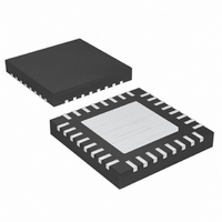
MAX5072ETJ+ Maxim Integrated Products, MAX5072ETJ+ Datasheet - Page 15

MAX5072ETJ+
Manufacturer Part Number
MAX5072ETJ+
Description
IC CONV BUCK/BOOST 32-TQFN
Manufacturer
Maxim Integrated Products
Type
Step-Down (Buck), Step-Up (Boost)r
Datasheet
1.MAX5072ETJ.pdf
(27 pages)
Specifications of MAX5072ETJ+
Internal Switch(s)
Yes
Synchronous Rectifier
No
Number Of Outputs
2
Voltage - Output
0.8 ~ 28 V
Current - Output
1A, 2A
Frequency - Switching
200kHz ~ 2.2MHz
Voltage - Input
4.5 ~ 23 V
Operating Temperature
-40°C ~ 85°C
Mounting Type
Surface Mount
Package / Case
32-TQFN Exposed Pad
Power - Output
2.76W
Output Voltage
5.2 V
Output Current
2 A
Input Voltage
5.5 V to 23 V
Supply Current
2.2 mA
Switching Frequency
1250 KHz
Mounting Style
SMD/SMT
Maximum Operating Temperature
+ 85 C
Minimum Operating Temperature
- 40 C
Lead Free Status / RoHS Status
Lead free / RoHS Compliant
All internal control circuitry operates from an internally
regulated nominal voltage of 5.2V (VL). At higher input
voltages (V+) of 5.5V to 23V, VL is regulated to 5.2V. At
5.5V or below, the internal linear regulator operates in
dropout mode, where VL follows V+. Depending on the
load on VL, the dropout voltage can be high enough to
reduce VL below the undervoltage lockout (UVLO)
threshold.
For input voltages of less than 5.5V, connect V+ and VL
together. The load on VL is proportional to the switch-
ing frequency of converter 1 and converter 2. See the
VL Dropout Voltage vs. Each Converter Switching
Frequency graph in the Typical Operating
Characteristics. For input voltage ranges higher than
5.5V, use the internal regulator.
Bypass V+ to SGND with a low-ESR, 0.1µF or greater
ceramic capacitor placed close to the MAX5072. Current
spikes from VL may disturb internal circuitry powered by
VL. Bypass VL with a low-ESR, ceramic 0.1µF capacitor
to PGND and a 4.7µF capacitor to SGND.
The MAX5072 includes an undervoltage lockout with
hysteresis and a power-on-reset circuit for smooth con-
verter turn-on and monotonic rise of the output voltage.
The rising UVLO threshold is internally set to 4.3V with
a 175mV hysteresis. Hysteresis at UVLO eliminates
“chattering” during startup. When VL drops below
UVLO, the internal switches are turned off and RST is
forced low.
Digital soft-start/soft-stop is provided internally to
reduce input surge currents and glitches at the input
during turn-on/turn-off. When UVLO is cleared and EN_
is high, digital soft-start slowly ramps up the internal
reference voltage in 64 steps. The total soft-start period
is 2048 switching cycles of the internal oscillator.
To calculate the soft-start period, use the following
equation:
where f
which is twice the switching frequency of each converter.
OSC
Input Voltage (V+)/Internal Linear
is the internal oscillator frequency in hertz,
Converter with POR and Power-Fail Output
Undervoltage Lockout/Soft-Start
______________________________________________________________________________________
t
SS
=
2048
f
OSC
2.2MHz, Dual-Output Buck or Boost
Regulator (VL)
The MAX5072 dual converter provides separate enable
inputs EN1 and EN2 to individually control or sequence
the output voltages. These active-high enable inputs are
TTL compatible. Pulling EN_ high ramps up the reference
slowly, which provides soft-start at the outputs. Forcing
the EN_ low externally disables the individual output and
generates a RST signal. Use EN1, EN2, and PGOOD1 for
sequencing (see Figure 4). Connect PGOOD1 to EN2 to
make sure converter 1’s output is within regulation before
converter 2 starts. Add an RC network from VL to EN1
and EN2 to delay the individual converter. A larger RC
time constant means a more delayed output. Sequencing
reduces input inrush current and possible chattering.
Connect the EN_ to VL for always-on operation.
Microprocessor-based products require manual reset
capability, allowing the operator or external logic circuitry
to initiate a reset. A logic low on MR asserts reset. Reset
remains asserted while MR is low, and for the Reset
Active Timeout Period (t
has an internal 44kΩ pullup resistor to VL, so it can be
left unconnected if not used. MR can be driven to TTL
logic levels.
Connect a normally open momentary switch from MR to
SGND to create a manual reset function. Note that
external debounce circuitry is not required. If MR is dri-
ven from long cables or if the device is used in a noisy
environment, connect a 0.1µF capacitor from MR to
SGND to provide additional noise immunity.
RST is an open-drain output. RST pulls low when either
output falls below 92.5% of its nominal regulation volt-
age. Once both outputs exceed 92.5% of their nominal
regulated voltages and both soft-start cycles are com-
pleted, RST enters a high-impedance state after the
180ms active timeout period. To obtain a logic-voltage
output, connect a pullup resistor from RST to a logic
supply voltage. The internal open-drain MOSFET can
sink 3mA while providing a TTL logic-low signal. If
unused, ground RST or leave it unconnected.
In addition to RST, converter 1 also includes a power-
good flag. Pull PGOOD1 to a logic voltage to provide
logic-level output. PGOOD1 is an open-drain output and
can sink 3mA while providing the TTL logic-low
signal. PGOOD1 goes low when converter 1’s output
drops to 92.5% of its nominal regulated voltage. Connect
PGOOD1 to SGND or leave unconnected, if not used.
RP
) after MR returns high. MR
RST Output
PGOOD1
Enable
MR
15


