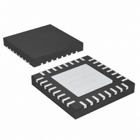
MAX5072ETJ+ Maxim Integrated Products, MAX5072ETJ+ Datasheet - Page 19

MAX5072ETJ+
Manufacturer Part Number
MAX5072ETJ+
Description
IC CONV BUCK/BOOST 32-TQFN
Manufacturer
Maxim Integrated Products
Type
Step-Down (Buck), Step-Up (Boost)r
Datasheet
1.MAX5072ETJ.pdf
(27 pages)
Specifications of MAX5072ETJ+
Internal Switch(s)
Yes
Synchronous Rectifier
No
Number Of Outputs
2
Voltage - Output
0.8 ~ 28 V
Current - Output
1A, 2A
Frequency - Switching
200kHz ~ 2.2MHz
Voltage - Input
4.5 ~ 23 V
Operating Temperature
-40°C ~ 85°C
Mounting Type
Surface Mount
Package / Case
32-TQFN Exposed Pad
Power - Output
2.76W
Output Voltage
5.2 V
Output Current
2 A
Input Voltage
5.5 V to 23 V
Supply Current
2.2 mA
Switching Frequency
1250 KHz
Mounting Style
SMD/SMT
Maximum Operating Temperature
+ 85 C
Minimum Operating Temperature
- 40 C
Lead Free Status / RoHS Status
Lead free / RoHS Compliant
ripple of 100mV or less, yielding an ESR and capaci-
tance value of 20mΩ and 6.8µF for 1.25MHz frequency.
Use a 100µF capacitor at low input voltages to avoid
possible undershoot below the undervoltage lockout
threshold during power-on and transient loading.
The allowable output ripple voltage and the maximum
deviation of the output voltage during step load currents
determines the output capacitance and its ESR.
The output ripple is comprised of ∆V
capacitor discharge) and ∆V
the capacitor). Use low-ESR ceramic or aluminum elec-
trolytic capacitors at the output. For aluminum electrolytic
capacitors, the entire output ripple is contributed by
∆V
requirement and choose the capacitor accordingly. If
using ceramic capacitors, assume the contribution to
the output ripple voltage from the ESR and the capacitor
discharge are equal. Calculate the output capacitance
and ESR required for a specified ripple using the follow-
ing equations:
where
where ∆I
culated above and f
switching frequency.
The allowable deviation of the output voltage during
fast transient loads also determines the output capaci-
tance and its ESR. The output capacitor supplies the
step load current until the controller responds with a
greater duty cycle. The response time (t
depends on the closed-loop bandwidth of the convert-
er. The high switching frequency of MAX5072 allows for
higher closed-loop bandwidth, reducing t
and the output capacitance requirement. The resistive
drop across the output capacitor ESR and the capaci-
tor discharge causes a voltage droop during a step
load. Use a combination of low-ESR tantalum and
ceramic capacitors for better transient load and
ripple/noise performance. Keep the maximum output
voltage deviation above the tolerable limits of the elec-
ESR
. Use the ESR
L
is the peak-to-peak inductor current as cal-
Converter with POR and Power-Fail Output
∆
C
V
O RIPPLE
OUT
_
______________________________________________________________________________________
ESR
OUT
=
SW
OUT
8
equation to calculate the ESR
×
is the individual converter’s
Output Capacitor Selection
≅
=
∆
ESR
∆
V
V
∆
∆
2.2MHz, Dual-Output Buck or Boost
Q
ESR
V
I
∆
L
ESR
(caused by the ESR of
I
×
L
+
f
SW
∆
Q
V
Q
(caused by the
RESPONSE
RESPONSE
)
tronics being powered. When using a ceramic capaci-
tor, assume 80% and 20% contribution from the output
capacitance discharge and the ESR drop, respectively.
Use the following equations to calculate the required
ESR and capacitance value:
where I
response time of the controller. Controller response
time depends on the control-loop bandwidth.
The MAX5072 can be configured for step-up conversion
since the internal MOSFET can be used as a low-side
switch. Use the following equations to calculate the
inductor (L
itor (C
Choose the minimum inductor value so the converter
remains in continuous mode operation at minimum out-
put current (I
where
and I
The V
diode, D is the duty cycle, and V
across the internal switch. Select the inductor with low DC
resistance and with a saturation current (I
er than the peak switch current limit of 4.5A and 2.2A of
converter 1 and converter 2, respectively.
The input current for the boost converter is continuous
and the RMS ripple current at the input is low. Calculate
the capacitor value and ESR of the input capacitor
using the following equations.
OMIN
D
OUT
is the forward voltage drop of the external Schottky
STEP
) when using the converter in boost operation.
MIN
L
= 0.25 x I
MIN
C
OMIN
is the load step and t
OUT
), input capacitor (C
=
D
ESR
).
2
=
=
O
×
I
STEP
V
V
OUT
O
O
V
f
SW
2
+
+
IN
V
V
=
×
D
D
×
×
∆
∆
I
−
−
STEP
t
V
V
RESPONSE
V
D
Q
V
V
ESR
O
IN
DS
DS
IN
×
Boost Converter
×
), and output capac-
η
is the voltage drop
I
RESPONSE
OMIN
Input Capacitor
SAT
) rating high-
Inductor
is the
19


