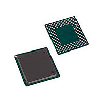
IDT72V51333L7-5BB8 IDT, Integrated Device Technology Inc, IDT72V51333L7-5BB8 Datasheet - Page 11

IDT72V51333L7-5BB8
Manufacturer Part Number
IDT72V51333L7-5BB8
Description
IC FLOW CTRL MULTI QUEUE 256-BGA
Manufacturer
IDT, Integrated Device Technology Inc
Datasheet
1.IDT72V51333L7-5BB8.pdf
(49 pages)
Specifications of IDT72V51333L7-5BB8
Configuration
Dual
Density
512Kb
Access Time (max)
4ns
Word Size
18b
Organization
4Kx18x8
Sync/async
Synchronous
Expandable
Yes
Bus Direction
Uni-Directional
Package Type
BGA
Clock Freq (max)
133MHz
Operating Supply Voltage (typ)
3.3V
Operating Supply Voltage (min)
3.15V
Operating Supply Voltage (max)
3.45V
Supply Current
100mA
Operating Temp Range
0C to 70C
Operating Temperature Classification
Commercial
Mounting
Surface Mount
Pin Count
256
Lead Free Status / RoHS Status
Contains lead / RoHS non-compliant
Other names
72V51333L7-5BB8
NOTE:
1. Stresses greater than those listed under ABSOLUTE MAXIMUM RATINGS may cause
NOTES
1. Measurements with 0.4 ≤ V
2. OE
3. Tested with outputs open (I
4. RCLK and WCLK toggle at 20 MHz and data inputs switch at 10 MHz.
5. Typical I
6. RCLK and WCLK, toggle at 20 MHz.
ABSOLUTE MAXIMUM RATINGS
CAPACITANCE
DC ELECTRICAL CHARACTERISTICS
(Commercial: V
NOTES:
1. With output deselected, (OE ≥ V
2. Characterized values, not currently tested.
IDT72V51333/72V51343/72V51353 3.3V, MULTI-QUEUE FLOW-CONTROL DEVICES
(8 QUEUES) 18 BIT WIDE CONFIGURATION 589,824, 1,179,648 and 2,359,296 bits
Symbol
C
C
V
T
I
permanent damage to the device. This is a stress rating only and functional operation
of the device at these or any other conditions above those indicated in the operational
sections of this specification is not implied. Exposure to absolute maximum rating
conditions for extended periods may affect reliability.
C
The following inputs should be pulled to GND: WRADD, RDADD, WADEN, RADEN, FSTR, ESTR, SCLK, SI, EXI, FXI and all Data Inputs.
The following inputs should be pulled to V
All other inputs are don't care, and should be pulled HIGH or LOW.
Symbol
I
I
V
V
I
I
IN
OUT
OUT
LI
LO
CC1
CC2
Symbol
STG
L
TERM
OH
OL
(2)
(1)
(2)
= capacitive load (in pF).
≥
:
(1,2)
(3,4,5)
(3,6)
V
IH,
CC1
0.4 ≤ V
= 16 + 3.14*f
CC
Parameter
Input Leakage Current
Output Leakage Current
Output Logic “1” Voltage, I
Output Logic “0” Voltage, I
Active Power Supply Current
Standby Current
Capacitance
Capacitance
OUT
Terminal Voltage
with respect to GND
Storage Temperature
DC Output Current
= 3.3V ± 0.15V, T
Output
Input
≤ V
CC.
S
Rating
OUT
+ 0.02*C
(1)
IN
≤ V
(T
= 0).
IH
A
CC
).
= +25°C, f = 1.0MHz)
L
.
*f
S
Conditions
A
V
(in mA) with V
V
= 0°C to +70°C;Industrial: V
OUT
CC
IN
OH
OL
: WEN, REN, SENI, PRS, MRS, TDI, TMS and TRST.
= 0V
= 0V
Parameter
= 8 mA
= –8 mA
Com'l & Ind'l
–0.5 to +4.5
–55 to +125
–50 to +50
CC
= 3.3V, t
Max.
10
10
A
= 25
Unit
°
Unit
°
mA
CC
pF
pF
V
C, f
C
= 3.3V ± 0.15V, T
S
= WCLK frequency = RCLK frequency (in MHz, using TTL levels), data switching at f
11
RECOMMENDED DC OPERATING
CONDITIONS
NOTE:
1. V
Symbol
V
GND
V
V
CC
T
T
CC
IH
IL
A
A
(1)
= 3.3V ± 0.15V, JEDEC JESD8-A compliant.
A
Supply Voltage (Com'l/Ind'l)
Supply Voltage (Com'l/Ind'l)
Input High Voltage (Com'l/Ind'l)
Input Low Voltage (Com'l/Ind'l)
Operating Temperature Commercial
Operating Temperature Industrial
= 40°C to +85°C; JEDEC JESD8-A compliant)
Min.
Parameter
–10
–10
2.4
—
—
—
COMMERCIAL AND INDUSTRIAL
Max.
100
0.4
10
10
—
25
TEMPERATURE RANGES
Min.
3.15
2.0
-40
—
0
0
Typ.
3.3
—
—
—
—
0
V
CC
Max.
3.45
+70
+85
0.8
0
+0.3
Unit
mA
mA
µA
µA
V
V
S
Unit
/2,
°
°
V
V
V
V
C
C


