ADC1415S125/DB,598 NXP Semiconductors, ADC1415S125/DB,598 Datasheet - Page 22
ADC1415S125/DB,598
Manufacturer Part Number
ADC1415S125/DB,598
Description
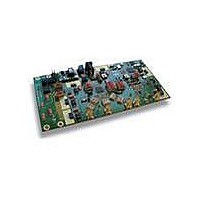
BOARD DEMO FOR ADC1415S125
Manufacturer
NXP Semiconductors
Type
A/Dr
Datasheets
1.ADC1415S125HNC15.pdf
(42 pages)
2.HSDC-ACC01DB.pdf
(32 pages)
3.ADC1415S125DB598.pdf
(2 pages)
Specifications of ADC1415S125/DB,598
Number Of Adc's
1
Number Of Bits
14
Sampling Rate (per Second)
125M
Data Interface
Serial, SPI™
Inputs Per Adc
1 Differential
Input Range
1 ~ 2 Vpp
Power (typ) @ Conditions
840mW @ 125Msps
Voltage Supply Source
Single Supply
Operating Temperature
-40°C ~ 85°C
Utilized Ic / Part
ADC1415S125
Product
Data Conversion Development Tools
Conversion Rate
125 MSPS
Resolution
14 bit
Interface Type
SMA
For Use With/related Products
ADC1415S125
Lead Free Status / RoHS Status
Lead free / RoHS Compliant
Lead Free Status / RoHS Status
Lead free / RoHS Compliant, Lead free / RoHS Compliant
Other names
568-5094


NXP Semiconductors
ADC1415S_SER
Product data sheet
Fig 18. Internal reference, 2 V (p-p) full scale
Fig 20. External reference, 1 V (p-p) to 2 V (p-p)
full-scale
11.3.2 Programmable full-scale
11.3.3 Common-mode output voltage (V
11.3.4 Biasing
V
330 pF
SENSE
VREF
VDDA
0.1 μF
SENSE
Figure 18
required reference voltage source.
The full-scale is programmable between 1 V (peak-to-peak) to 2 V (peak-to-peak)
(see
Table 12.
A 0.1 μF filter capacitor should be connected between pin VCM and ground.
The common-mode input voltage (V
buffer bias current can be set to one of three levels (high, medium or low) via the SPI (see
Table
VREF
INTREF
000
001
010
011
100
101
110
111
EQUIVALENT
REFERENCE
Table
SCHEMATIC
22).
REFERENCE
EQUIVALENT
SCHEMATIC
to
Reference SPI Gain Control
12).
005aaa116
Figure 21
005aaa119
All information provided in this document is subject to legal disclaimers.
Single 14-bit ADC; input buffer; CMOS or LVDS DDR digital outputs
Rev. 4 — 17 December 2010
illustrate how to connect the SENSE and VREF pins to select the
Gain
0 dB
−1 dB
−2 dB
−3 dB
−4 dB
−5 dB
−6 dB
reserved
Fig 19. Internal reference, 1 V (p-p) full scale
Fig 21. Internal reference via SPI, 1 V (p-p) to 2 V (p-p)
I(cm)
O(cm)
) on pins INP and INM is set internally. The input
full-scale
)
330 pF
330
pF
Full-scale (p-p)
2 V
1.78 V
1.59 V
1.42 V
1.26 V
1.12 V
1 V
x
ADC1415S series
SENSE
SENSE
VREF
VREF
EQUIVALENT
REFERENCE
SCHEMATIC
EQUIVALENT
REFERENCE
SCHEMATIC
005aaa117
005aaa118
© NXP B.V. 2010. All rights reserved.
22 of 42
Related parts for ADC1415S125/DB,598
Image
Part Number
Description
Manufacturer
Datasheet
Request
R

Part Number:
Description:
Single 14-bit ADC
Manufacturer:
NXP Semiconductors
Datasheet:
Part Number:
Description:
NXP Semiconductors designed the LPC2420/2460 microcontroller around a 16-bit/32-bitARM7TDMI-S CPU core with real-time debug interfaces that include both JTAG andembedded trace
Manufacturer:
NXP Semiconductors
Datasheet:

Part Number:
Description:
NXP Semiconductors designed the LPC2458 microcontroller around a 16-bit/32-bitARM7TDMI-S CPU core with real-time debug interfaces that include both JTAG andembedded trace
Manufacturer:
NXP Semiconductors
Datasheet:
Part Number:
Description:
NXP Semiconductors designed the LPC2468 microcontroller around a 16-bit/32-bitARM7TDMI-S CPU core with real-time debug interfaces that include both JTAG andembedded trace
Manufacturer:
NXP Semiconductors
Datasheet:
Part Number:
Description:
NXP Semiconductors designed the LPC2470 microcontroller, powered by theARM7TDMI-S core, to be a highly integrated microcontroller for a wide range ofapplications that require advanced communications and high quality graphic displays
Manufacturer:
NXP Semiconductors
Datasheet:
Part Number:
Description:
NXP Semiconductors designed the LPC2478 microcontroller, powered by theARM7TDMI-S core, to be a highly integrated microcontroller for a wide range ofapplications that require advanced communications and high quality graphic displays
Manufacturer:
NXP Semiconductors
Datasheet:
Part Number:
Description:
The Philips Semiconductors XA (eXtended Architecture) family of 16-bit single-chip microcontrollers is powerful enough to easily handle the requirements of high performance embedded applications, yet inexpensive enough to compete in the market for hi
Manufacturer:
NXP Semiconductors
Datasheet:
Part Number:
Description:
The XA-S3 device is a member of Philips Semiconductors? XA(eXtended Architecture) family of high performance 16-bitsingle-chip microcontrollers
Manufacturer:
NXP Semiconductors
Datasheet:

Part Number:
Description:
The NXP BlueStreak LH75401/LH75411 family consists of two low-cost 16/32-bit System-on-Chip (SoC) devices
Manufacturer:
NXP Semiconductors
Datasheet:
Part Number:
Description:
The NXP LPC3130/3131 combine an 180 MHz ARM926EJ-S CPU core, high-speed USB2
Manufacturer:
NXP Semiconductors
Datasheet:
Part Number:
Description:
The NXP LPC3141 combine a 270 MHz ARM926EJ-S CPU core, High-speed USB 2
Manufacturer:
NXP Semiconductors
Part Number:
Description:
The NXP LPC3143 combine a 270 MHz ARM926EJ-S CPU core, High-speed USB 2
Manufacturer:
NXP Semiconductors

Part Number:
Description:
The NXP LPC3152 combines an 180 MHz ARM926EJ-S CPU core, High-speed USB 2
Manufacturer:
NXP Semiconductors
Part Number:
Description:
The NXP LPC3154 combines an 180 MHz ARM926EJ-S CPU core, High-speed USB 2
Manufacturer:
NXP Semiconductors