ADC1415S125/DB,598 NXP Semiconductors, ADC1415S125/DB,598 Datasheet - Page 4
ADC1415S125/DB,598
Manufacturer Part Number
ADC1415S125/DB,598
Description
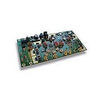
BOARD DEMO FOR ADC1415S125
Manufacturer
NXP Semiconductors
Type
A/Dr
Datasheets
1.ADC1415S125HNC15.pdf
(42 pages)
2.HSDC-ACC01DB.pdf
(32 pages)
3.ADC1415S125DB598.pdf
(2 pages)
Specifications of ADC1415S125/DB,598
Number Of Adc's
1
Number Of Bits
14
Sampling Rate (per Second)
125M
Data Interface
Serial, SPI™
Inputs Per Adc
1 Differential
Input Range
1 ~ 2 Vpp
Power (typ) @ Conditions
840mW @ 125Msps
Voltage Supply Source
Single Supply
Operating Temperature
-40°C ~ 85°C
Utilized Ic / Part
ADC1415S125
Product
Data Conversion Development Tools
Conversion Rate
125 MSPS
Resolution
14 bit
Interface Type
SMA
For Use With/related Products
ADC1415S125
Lead Free Status / RoHS Status
Lead free / RoHS Compliant
Lead Free Status / RoHS Status
Lead free / RoHS Compliant, Lead free / RoHS Compliant
Other names
568-5094


NXP Semiconductors
6. Pinning information
ADC1415S_SER
Product data sheet
Fig 2.
index area
terminal 1
VDDA5V
VDDA3V
AGND
AGND
AGND
REFB
REFT
Pin configuration with CMOS digital outputs
selected
VCM
INM
INP
10
1
2
3
4
5
6
7
8
9
6.1 Pinning
6.2 Pin description
Table 2.
Symbol
REFB
REFT
AGND
VCM
VDDA5V
AGND
INM
INP
AGND
VDDA3V
VDDA3V
CLKP
CLKM
DEC
OE
PWD
Transparent top view
ADC1415S
HVQFN40
Pin description (CMOS digital outputs)
Pin
1
2
3
4
5
6
7
8
9
10
11
12
13
14
15
16
All information provided in this document is subject to legal disclaimers.
Single 14-bit ADC; input buffer; CMOS or LVDS DDR digital outputs
005aaa102
Type
O
O
G
O
P
G
I
I
G
P
P
I
I
O
I
I
Rev. 4 — 17 December 2010
30
29
28
27
26
25
24
23
22
21
D0
D1
D2
D3
D4
D5
D6
D7
D8
D9
[1]
Fig 3.
Description
bottom reference
top reference
analog ground
common-mode output voltage
5 V analog power supply
analog ground
complementary analog input
analog input
analog ground
3 V analog power supply
3 V analog power supply
clock input
complementary clock input
regulator decoupling node
output enable, active LOW
power down, active HIGH
index area
terminal 1
VDDA5V
VDDA3V
AGND
AGND
AGND
REFB
REFT
VCM
INM
INP
Pin configuration with LVDS/DDR digital
outputs selected
10
1
2
3
4
5
6
7
8
9
ADC1415S series
Transparent top view
ADC1215S
HVQFN40
© NXP B.V. 2010. All rights reserved.
30
29
28
27
26
25
24
23
22
21
005aaa103
D0_D1_P
D0_D1_M
D2_D3_P
D2_D3_M
D4_D5_P
D4_D5_M
D6_D7_P
D6_D7_M
D8_D9_P
D8_D9_M
4 of 42
Related parts for ADC1415S125/DB,598
Image
Part Number
Description
Manufacturer
Datasheet
Request
R

Part Number:
Description:
Single 14-bit ADC
Manufacturer:
NXP Semiconductors
Datasheet:
Part Number:
Description:
NXP Semiconductors designed the LPC2420/2460 microcontroller around a 16-bit/32-bitARM7TDMI-S CPU core with real-time debug interfaces that include both JTAG andembedded trace
Manufacturer:
NXP Semiconductors
Datasheet:

Part Number:
Description:
NXP Semiconductors designed the LPC2458 microcontroller around a 16-bit/32-bitARM7TDMI-S CPU core with real-time debug interfaces that include both JTAG andembedded trace
Manufacturer:
NXP Semiconductors
Datasheet:
Part Number:
Description:
NXP Semiconductors designed the LPC2468 microcontroller around a 16-bit/32-bitARM7TDMI-S CPU core with real-time debug interfaces that include both JTAG andembedded trace
Manufacturer:
NXP Semiconductors
Datasheet:
Part Number:
Description:
NXP Semiconductors designed the LPC2470 microcontroller, powered by theARM7TDMI-S core, to be a highly integrated microcontroller for a wide range ofapplications that require advanced communications and high quality graphic displays
Manufacturer:
NXP Semiconductors
Datasheet:
Part Number:
Description:
NXP Semiconductors designed the LPC2478 microcontroller, powered by theARM7TDMI-S core, to be a highly integrated microcontroller for a wide range ofapplications that require advanced communications and high quality graphic displays
Manufacturer:
NXP Semiconductors
Datasheet:
Part Number:
Description:
The Philips Semiconductors XA (eXtended Architecture) family of 16-bit single-chip microcontrollers is powerful enough to easily handle the requirements of high performance embedded applications, yet inexpensive enough to compete in the market for hi
Manufacturer:
NXP Semiconductors
Datasheet:
Part Number:
Description:
The XA-S3 device is a member of Philips Semiconductors? XA(eXtended Architecture) family of high performance 16-bitsingle-chip microcontrollers
Manufacturer:
NXP Semiconductors
Datasheet:

Part Number:
Description:
The NXP BlueStreak LH75401/LH75411 family consists of two low-cost 16/32-bit System-on-Chip (SoC) devices
Manufacturer:
NXP Semiconductors
Datasheet:
Part Number:
Description:
The NXP LPC3130/3131 combine an 180 MHz ARM926EJ-S CPU core, high-speed USB2
Manufacturer:
NXP Semiconductors
Datasheet:
Part Number:
Description:
The NXP LPC3141 combine a 270 MHz ARM926EJ-S CPU core, High-speed USB 2
Manufacturer:
NXP Semiconductors
Part Number:
Description:
The NXP LPC3143 combine a 270 MHz ARM926EJ-S CPU core, High-speed USB 2
Manufacturer:
NXP Semiconductors

Part Number:
Description:
The NXP LPC3152 combines an 180 MHz ARM926EJ-S CPU core, High-speed USB 2
Manufacturer:
NXP Semiconductors
Part Number:
Description:
The NXP LPC3154 combines an 180 MHz ARM926EJ-S CPU core, High-speed USB 2
Manufacturer:
NXP Semiconductors