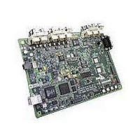
AD9204-20EBZ Analog Devices Inc, AD9204-20EBZ Datasheet - Page 25

AD9204-20EBZ
Manufacturer Part Number
AD9204-20EBZ
Description
BOARD EVALUATION 20MSPS AD9204
Manufacturer
Analog Devices Inc
Datasheet
1.AD9204BCPZ-20.pdf
(36 pages)
Specifications of AD9204-20EBZ
Number Of Adc's
2
Number Of Bits
10
Sampling Rate (per Second)
20M
Data Interface
Serial, SPI™
Inputs Per Adc
1 Differential
Input Range
1 ~ 2 Vpp
Power (typ) @ Conditions
*
Voltage Supply Source
Single Supply
Operating Temperature
-40°C ~ 85°C
Utilized Ic / Part
AD9204
Silicon Manufacturer
Analog Devices
Application Sub Type
ADC
Kit Application Type
Data Converter
Silicon Core Number
AD9204
Tool / Board Applications
General Purpose MCU, MPU, DSP, DSC
Development Tool Type
Hardware / Software - Starter Kit
Lead Free Status / RoHS Status
Lead free / RoHS Compliant
Jitter Considerations
High speed, high resolution ADCs are sensitive to the quality
of the clock input. The degradation in SNR from the low fre-
quency SNR (SNR
jitter (t
In the previous equation, the rms aperture jitter represents
the clock input jitter specification. Input frequency (IF)
undersampling applications are particularly sensitive to jitter,
as illustrated in Figure 56.
The clock input should be treated as an analog signal in cases in
which aperture jitter may affect the dynamic range of the AD9204.
To avoid modulating the clock signal with digital noise, keep
power supplies for clock drivers separate from the ADC output
driver supplies. Low jitter, crystal-controlled oscillators make
the best clock sources. If the clock is generated from another type
of source (by gating, dividing, or another method), it should be
retimed by the original clock at the last step.
See the AN-501 Application Note and the AN-756 Application
Note available on
SNR
80
75
70
65
60
55
50
45
JRMS
1
HF
) can be calculated by
= −10 log[(2π × f
Figure 56. SNR vs. Input Frequency and Jitter
www.analog.com
LF
) at a given input frequency (f
10
FREQUENCY (MHz)
INPUT
× t
for more information.
JRMS
)
100
2
+ 10
3.0ps
(
−
SNR
0.05ps
0.2ps
0.5ps
1.0ps
1.5ps
2.0ps
2.5ps
INPUT
LF
/
10
) due to
)
1k
]
Rev. 0 | Page 25 of 36
POWER DISSIPATION AND STANDBY MODE
As shown in Figure 57, the analog core power dissipated by
the AD9204 is proportional to its sample rate. The digital
power dissipation of the CMOS outputs is determined primarily
by the strength of the digital drivers and the load
on each output bit.
The maximum DRVDD current (IDRVDD) can be calculated as
where N is the number of output bits (30, in the case of the
AD9204).
This maximum current occurs when every output bit switches
on every clock cycle, that is, a full-scale square wave at the Nyquist
frequency of f
lished by the average number of output bits switching, which
is determined by the sample rate and the characteristics of the
analog input signal.
Reducing the capacitive load presented to the output drivers can
minimize digital power consumption. The data in Figure 57 was
taken using the same operating conditions as those used in the
Typical Performance Characteristics, with a 5 pF load on each
output driver.
IDRVDD = V
140
130
120
110
100
90
80
70
60
50
0
Figure 57. AD9204 Analog Core Power vs. Clock Rate
CLK
10
/2. In practice, the DRVDD current is estab-
DRVDD
20
× C
AD9204-20
CLOCK RATE (MSPS)
30
LOAD
× f
AD9204-40
40
CLK
AD9204-80
× N
50
AD9204-65
60
70
AD9204
80


