AD9204-20EBZ Analog Devices Inc, AD9204-20EBZ Datasheet - Page 30
AD9204-20EBZ
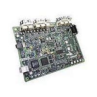
Manufacturer Part Number
AD9204-20EBZ
Description
BOARD EVALUATION 20MSPS AD9204
Manufacturer
Analog Devices Inc
Datasheet
1.AD9204BCPZ-20.pdf
(36 pages)
Specifications of AD9204-20EBZ
Number Of Adc's
2
Number Of Bits
10
Sampling Rate (per Second)
20M
Data Interface
Serial, SPI™
Inputs Per Adc
1 Differential
Input Range
1 ~ 2 Vpp
Power (typ) @ Conditions
*
Voltage Supply Source
Single Supply
Operating Temperature
-40°C ~ 85°C
Utilized Ic / Part
AD9204
Silicon Manufacturer
Analog Devices
Application Sub Type
ADC
Kit Application Type
Data Converter
Silicon Core Number
AD9204
Tool / Board Applications
General Purpose MCU, MPU, DSP, DSC
Development Tool Type
Hardware / Software - Starter Kit
Lead Free Status / RoHS Status
Lead free / RoHS Compliant


AD9204
HARDWARE INTERFACE
The pins described in Table 14 constitute the physical interface
between the programming device of the user and the serial port
of the AD9204. The SCLK and CSB pins function as inputs
when using the SPI interface. The SDIO pin is bidirectional,
functioning as an input during write phases and as an output
during readback.
The SPI interface is flexible enough to be controlled by
either FPGAs or microcontrollers. One method for SPI
configuration is described in detail in the AN-812 Appli-
cation Note, Microcontroller-Based Serial Port Interface
(SPI) Boot Circuit.
The SPI port should not be active during periods when the full
dynamic performance of the converter is required. Because the
SCLK signal, the CSB signal, and the SDIO signal are typically
asynchronous to the ADC clock, noise from these signals can
degrade converter performance. If the on-board SPI bus is used
for other devices, it may be necessary to provide buffers between
this bus and the AD9204 to prevent these signals from transi-
tioning at the converter inputs during critical sampling periods.
SDIO/DCS and SCLK/DFS serve a dual function when the
SPI interface is not being used. When the pins are strapped to
AVDD or ground during device power-on, they are associated
with a specific function. The Digital Outputs section describes
the strappable functions supported on the AD9204.
CONFIGURATION WITHOUT THE SPI
In applications that do not interface to the SPI control registers,
the SDIO/DCS pin, the SCLK/DFS pin, the OEB pin, and the
PDWN pin serve as standalone CMOS-compatible control
pins. When the device is powered up, it is assumed that the
user intends to use the pins as static control lines for the duty
cycle stabilizer, output data format, output enable, and power-
down feature control. In this mode, connect the CSB chip
select to AVDD, which disables the serial port interface.
Rev. 0 | Page 30 of 36
Table 15. Mode Selection
Pin
SDIO/DCS
SCLK/DFS
OEB
PDWN
SPI ACCESSIBLE FEATURES
Table 16 provides a brief description of the general features that
are accessible via the SPI. These features are described in detail
in the AN-877 Application Note, Interfacing to High Speed ADCs
via SPI. The AD9204 part-specific features are described in
detail in Table 17.
Table 16. Features Accessible Using the SPI
Feature
Mode
Clock
Offset
Test I/O
Output Mode
Output Phase
Output Delay
VREF
External
Voltage
AVDD (default)
AGND
AVDD
AGND (default)
AVDD
AGND (default)
AVDD
AGND (default)
Allows the user to vary the DCO delay
Description
Allows the user to set either power-down mode
or standby mode
Allows the user to access the DCS via the SPI
Allows the user to digitally adjust the
converter offset
Allows the user to set test modes to have known
data on output bits
Allows the user to set up outputs
Allows the user to set the output clock polarity
Allows the user to set the reference voltage
Configuration
Duty cycle stabilizer enabled
Duty cycle stabilizer disabled
Twos complement enabled
Offset binary enabled
Outputs in high impedance
Outputs enabled
Chip in power-down or standby
Normal operation
Related parts for AD9204-20EBZ
Image
Part Number
Description
Manufacturer
Datasheet
Request
R

Part Number:
Description:
10 Bit 40 Msps Dual Low Power ADC
Manufacturer:
Analog Devices Inc
Datasheet:
Part Number:
Description:
10 Bit 65 Msps Dual Low Power ADC
Manufacturer:
Analog Devices Inc
Datasheet:
Part Number:
Description:
10 Bit 80 Msps Dual Low Power ADC
Manufacturer:
Analog Devices Inc
Datasheet:

Part Number:
Description:
±1.7g Dual-Axis IMEMS Accelerometer Evaluation Board
Manufacturer:
Analog Devices Inc
Datasheet:
Part Number:
Description:
Inertial Sensor Evaluation System
Manufacturer:
Analog Devices Inc
Datasheet:
Part Number:
Description:
Manufacturer:
Analog Devices Inc
Datasheet:
Part Number:
Description:
Manufacturer:
Analog Devices Inc
Datasheet:
Part Number:
Description:
Manufacturer:
Analog Devices Inc
Datasheet:
Part Number:
Description:
Manufacturer:
Analog Devices Inc
Datasheet:
Part Number:
Description:
Manufacturer:
Analog Devices Inc
Datasheet:
Part Number:
Description:
Manufacturer:
Analog Devices Inc
Datasheet:
Part Number:
Description:
Manufacturer:
Analog Devices Inc
Datasheet:
Part Number:
Description:
Manufacturer:
Analog Devices Inc
Datasheet: