AD9204-20EBZ Analog Devices Inc, AD9204-20EBZ Datasheet - Page 29
AD9204-20EBZ
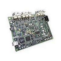
Manufacturer Part Number
AD9204-20EBZ
Description
BOARD EVALUATION 20MSPS AD9204
Manufacturer
Analog Devices Inc
Datasheet
1.AD9204BCPZ-20.pdf
(36 pages)
Specifications of AD9204-20EBZ
Number Of Adc's
2
Number Of Bits
10
Sampling Rate (per Second)
20M
Data Interface
Serial, SPI™
Inputs Per Adc
1 Differential
Input Range
1 ~ 2 Vpp
Power (typ) @ Conditions
*
Voltage Supply Source
Single Supply
Operating Temperature
-40°C ~ 85°C
Utilized Ic / Part
AD9204
Silicon Manufacturer
Analog Devices
Application Sub Type
ADC
Kit Application Type
Data Converter
Silicon Core Number
AD9204
Tool / Board Applications
General Purpose MCU, MPU, DSP, DSC
Development Tool Type
Hardware / Software - Starter Kit
Lead Free Status / RoHS Status
Lead free / RoHS Compliant


SERIAL PORT INTERFACE (SPI)
The AD9204 serial port interface (SPI) allows the user to configure
the converter for specific functions or operations through a
structured register space provided inside the ADC. The SPI
gives the user added flexibility and customization, depending
on the application. Addresses are accessed via the serial port
and can be written to or read from via the port. Memory is
organized into bytes that can be further divided into fields,
which are documented in the Memory Map section. For
detailed operational information, see the AN-877 Applica-
tion Note, Interfacing to High Speed ADCs via SPI.
CONFIGURATION USING THE SPI
Three pins define the SPI of this ADC: the SCLK, the SDIO,
and the CSB (see Table 14). The SCLK (a serial clock) is used
to synchronize the read and write data presented from and to
the ADC. The SDIO (serial data input/output) is a dual-purpose
pin that allows data to be sent and read from the internal ADC
memory map registers. The CSB (chip select bar) is an active-
low control that enables or disables the read and write cycles.
Table 14. Serial Port Interface Pins
Pin
SCLK
SDIO
CSB
SCLK
SDIO
CSB
DON’T CARE
DON’T CARE
Function
Serial Clock. The serial shift clock input is used to
synchronize serial interface reads and writes.
Serial Data Input/Output. A dual-purpose pin that
typically serves as an input or an output, depending
on the instruction being sent and the relative position
in the timing frame.
Chip Select Bar. An active-low control that gates the read
and write cycles.
t
S
R/W
t
DS
W1
W0
t
DH
A12
t
HIGH
A11
Figure 58. Serial Port Interface Timing Diagram
t
LOW
A10
A9
Rev. 0 | Page 29 of 36
t
CLK
A8
A7
The falling edge of CSB, in conjunction with the rising edge of
SCLK, determines the start of the framing. An example of the
serial timing and its definitions can be found in Figure 58 and
Table 5.
Other modes involving the CSB are available. The CSB can be
held low indefinitely, which permanently enables the device;
this is called streaming. The CSB can stall high between bytes to
allow for additional external timing. When CSB is tied high, SPI
functions are placed in high impedance mode. This mode turns
on any SPI pin secondary functions.
During an instruction phase, a 16-bit instruction is transmitted.
Data follows the instruction phase, and its length is determined
by the W0 and W1 bits, as shown in Figure 58.
All data is composed of 8-bit words. The first bit of the first byte
in a multibyte serial data transfer frame indicates whether a read
command or a write command is issued. This allows the serial
data input/output (SDIO) pin to change direction from an input
to an output at the appropriate point in the serial frame.
In addition to word length, the instruction phase determines
whether the serial frame is a read or write operation, allowing
the serial port to be used both to program the chip and to read
the contents of the on-chip memory. If the instruction is a readback
operation, performing a readback causes the serial data input/
output (SDIO) pin to change direction from an input to an output
at the appropriate point in the serial frame.
Data can be sent in MSB-first mode or in LSB-first mode. MSB
first is the default on power-up and can be changed via the SPI
port configuration register. For more information about this
and other features, see the AN-877 Application Note, Interfacing
to High Speed ADCs via SPI.
D5
D4
D3
D2
D1
D0
t
H
DON’T CARE
AD9204
DON’T CARE
Related parts for AD9204-20EBZ
Image
Part Number
Description
Manufacturer
Datasheet
Request
R

Part Number:
Description:
10 Bit 40 Msps Dual Low Power ADC
Manufacturer:
Analog Devices Inc
Datasheet:
Part Number:
Description:
10 Bit 65 Msps Dual Low Power ADC
Manufacturer:
Analog Devices Inc
Datasheet:
Part Number:
Description:
10 Bit 80 Msps Dual Low Power ADC
Manufacturer:
Analog Devices Inc
Datasheet:

Part Number:
Description:
±1.7g Dual-Axis IMEMS Accelerometer Evaluation Board
Manufacturer:
Analog Devices Inc
Datasheet:
Part Number:
Description:
Inertial Sensor Evaluation System
Manufacturer:
Analog Devices Inc
Datasheet:
Part Number:
Description:
Manufacturer:
Analog Devices Inc
Datasheet:
Part Number:
Description:
Manufacturer:
Analog Devices Inc
Datasheet:
Part Number:
Description:
Manufacturer:
Analog Devices Inc
Datasheet:
Part Number:
Description:
Manufacturer:
Analog Devices Inc
Datasheet:
Part Number:
Description:
Manufacturer:
Analog Devices Inc
Datasheet:
Part Number:
Description:
Manufacturer:
Analog Devices Inc
Datasheet:
Part Number:
Description:
Manufacturer:
Analog Devices Inc
Datasheet:
Part Number:
Description:
Manufacturer:
Analog Devices Inc
Datasheet: