AD9204-20EBZ Analog Devices Inc, AD9204-20EBZ Datasheet - Page 9
AD9204-20EBZ
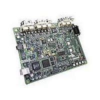
Manufacturer Part Number
AD9204-20EBZ
Description
BOARD EVALUATION 20MSPS AD9204
Manufacturer
Analog Devices Inc
Datasheet
1.AD9204BCPZ-20.pdf
(36 pages)
Specifications of AD9204-20EBZ
Number Of Adc's
2
Number Of Bits
10
Sampling Rate (per Second)
20M
Data Interface
Serial, SPI™
Inputs Per Adc
1 Differential
Input Range
1 ~ 2 Vpp
Power (typ) @ Conditions
*
Voltage Supply Source
Single Supply
Operating Temperature
-40°C ~ 85°C
Utilized Ic / Part
AD9204
Silicon Manufacturer
Analog Devices
Application Sub Type
ADC
Kit Application Type
Data Converter
Silicon Core Number
AD9204
Tool / Board Applications
General Purpose MCU, MPU, DSP, DSC
Development Tool Type
Hardware / Software - Starter Kit
Lead Free Status / RoHS Status
Lead free / RoHS Compliant


ABSOLUTE MAXIMUM RATINGS
Table 6.
Parameter
AVDD to AGND
DRVDD to AGND
VIN+A, VIN+B, VIN−A, VIN−B to AGND
CLK+, CLK− to AGND
SYNC to AGND
VREF to AGND
SENSE to AGND
VCM to AGND
RBIAS to AGND
CSB to AGND
SCLK/DFS to AGND
SDIO/DCS to AGND
OEB to AGND
PDWN to AGND
D0A/D0B Through D13A/D13B to AGND
DCOA/DCOB to AGND
Operating Temperature Range (Ambient)
Maximum Junction Temperature
Storage Temperature Range (Ambient)
Stresses above those listed under Absolute Maximum Ratings
may cause permanent damage to the device. This is a stress
rating only; functional operation of the device at these or any
other conditions above those indicated in the operational
section of this specification is not implied. Exposure to absolute
maximum rating conditions for extended periods may affect
device reliability.
Under Bias
Rating
−0.3 V to +2.0 V
−0.3 V to +3.9 V
−0.3 V to AVDD + 0.2 V
−0.3 V to AVDD + 0.2 V
−0.3 V to DRVDD + 0.3 V
−0.3 V to AVDD + 0.2 V
−0.3 V to AVDD + 0.2 V
−0.3 V to AVDD + 0.2 V
−0.3 V to AVDD + 0.2 V
−0.3 V to DRVDD + 0.3 V
−0.3 V to DRVDD + 0.3 V
−0.3 V to DRVDD + 0.3 V
−0.3 V to DRVDD + 0.3 V
−0.3 V to DRVDD + 0.3 V
−0.3 V to DRVDD + 0.3 V
−0.3 V to DRVDD + 0.3 V
−40°C to +85°C
150°C
−65°C to +150°C
Rev. 0 | Page 9 of 36
THERMAL CHARACTERISTICS
The exposed paddle is the only ground connection for the chip.
The exposed paddle must be soldered to the AGND plane of the
user’s circuit board. Soldering the exposed paddle to the user’s
board also increases the reliability of the solder joints and
maximizes the thermal capability of the package.
Table 7. Thermal Resistance
Package Type
64-Lead LFCSP
1
2
3
4
Typical θ
plane. As shown in Table 7, airflow improves heat dissipation,
which reduces θ
package leads from metal traces, through holes, ground, and
power planes reduces the θ
ESD CAUTION
Per JEDEC 51-7, plus JEDEC 25-5 2S2P test board.
Per JEDEC JESD51-2 (still air) or JEDEC JESD51-6 (moving air).
Per MIL-Std 883, Method 1012.1.
Per JEDEC JESD51-8 (still air).
9 mm × 9 mm
(CP-64-4)
JA
is specified for a 4-layer PCB with a solid ground
JA
. In addition, metal in direct contact with the
Airflow
Velocity
(m/sec)
0
1.0
2.5
JA
.
θ
23
20
18
JA
1, 2
θ
2.0
JC
1, 3
θ
12
AD9204
JB
1, 4
Unit
°C/W
°C/W
°C/W
Related parts for AD9204-20EBZ
Image
Part Number
Description
Manufacturer
Datasheet
Request
R

Part Number:
Description:
10 Bit 40 Msps Dual Low Power ADC
Manufacturer:
Analog Devices Inc
Datasheet:
Part Number:
Description:
10 Bit 65 Msps Dual Low Power ADC
Manufacturer:
Analog Devices Inc
Datasheet:
Part Number:
Description:
10 Bit 80 Msps Dual Low Power ADC
Manufacturer:
Analog Devices Inc
Datasheet:

Part Number:
Description:
±1.7g Dual-Axis IMEMS Accelerometer Evaluation Board
Manufacturer:
Analog Devices Inc
Datasheet:
Part Number:
Description:
Inertial Sensor Evaluation System
Manufacturer:
Analog Devices Inc
Datasheet:
Part Number:
Description:
Manufacturer:
Analog Devices Inc
Datasheet:
Part Number:
Description:
Manufacturer:
Analog Devices Inc
Datasheet:
Part Number:
Description:
Manufacturer:
Analog Devices Inc
Datasheet:
Part Number:
Description:
Manufacturer:
Analog Devices Inc
Datasheet:
Part Number:
Description:
Manufacturer:
Analog Devices Inc
Datasheet:
Part Number:
Description:
Manufacturer:
Analog Devices Inc
Datasheet:
Part Number:
Description:
Manufacturer:
Analog Devices Inc
Datasheet:
Part Number:
Description:
Manufacturer:
Analog Devices Inc
Datasheet: