CDB5532U Cirrus Logic Inc, CDB5532U Datasheet - Page 23
CDB5532U
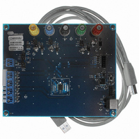
Manufacturer Part Number
CDB5532U
Description
BOARD EVAL FOR CS5532U ADC
Manufacturer
Cirrus Logic Inc
Specifications of CDB5532U
Number Of Adc's
2
Number Of Bits
24
Sampling Rate (per Second)
3.84k
Data Interface
Serial
Inputs Per Adc
1 Differential
Input Range
±2.5 V
Power (typ) @ Conditions
35mW @ 3.84kSPS
Voltage Supply Source
Analog and Digital, Dual ±
Operating Temperature
-40°C ~ 85°C
Utilized Ic / Part
CS5532
Description/function
Audio DSPs
Operating Supply Voltage
5 V
Product
Audio Modules
For Use With/related Products
C8051F320
Lead Free Status / RoHS Status
Contains lead / RoHS non-compliant
Lead Free Status / RoHS Status
Lead free / RoHS Compliant, Contains lead / RoHS non-compliant
Other names
598-1159


2.2.5. Reading/Writing On-Chip Registers
The CS5532/34’s offset, gain, configuration, and
channel-setup registers are readable and writable
while the conversion data register is read only.
As shown in Figure 7, to write to a particular regis-
ter the user must transmit the appropriate write
command and then follow that command by 32 bits
of data. For example, to write 0x80000000 (hexa-
decimal) to physical channel one’s gain register,
the user would first transmit the command byte
0x02 (hexadecimal) followed by the data
0x80000000 (hexadecimal). Similarly, to read a
particular register the user must transmit the appro-
priate read command and then acquire the 32 bits of
data. Once a register is written to or read from, the
serial port returns to the command mode.
In addition to accessing the internal registers one at
a time, the gain and offset registers as well as the
channel setup registers can be accessed as arrays
(i.e. the entire register set can be accessed with one
command). In the CS5532, there are two gain and
offset registers, and in the CS5534, there are four
gain and offset registers. There are four channel
setup registers in both devices. As an example, to
write 0x80000000 (hexadecimal) to all four gain
registers in the CS5534, the user would transmit the
command 0x42 (hexadecimal) followed by four it-
erations of 0x80000000 (hexadecimal), (i.e. 0x42
followed
0x80000000, 0x80000000). The registers are writ-
ten to or read from in sequential order (i.e, 1, fol-
lowed by 2, 3, and 4). Once the registers are written
to or read from, the serial port returns to the com-
mand mode.
2.3. Configuration Register
To ease the architectural design and simplify the
serial interface, the configuration register is thirty-
two bits long, however, only eleven of the thirty-
two bits are used. The following sections detail the
bits in the configuration register.
DS755F3
by
0x80000000,
0x80000000,
2.3.1. Power Consumption
The CS5532/34 accommodate three power con-
sumption modes: normal, standby, and sleep. The
default mode, “normal mode”, is entered after pow-
er is applied. In this mode, the CS5532/34-BS de-
vices typically consume 70 mW. The other two
modes are referred to as the power save modes.
They power down most of the analog portion of the
chip and stop filter convolutions. The power save
modes are entered whenever the power down
(PDW) bit of the configuration register is set to log-
ic 1. The particular power save mode entered de-
pends on state of the PSS (Power Save Select) bit.
If PSS is logic 0, the converter enters the standby
mode reducing the power consumption to 4 mW.
The standby mode leaves the oscillator and the on-
chip bias generator for the analog portion of the
chip active. This allows the converter to quickly re-
turn to the normal mode once PDW is set back to a
logic 1. If PSS and PDW are both set to logic 1, the
sleep mode is entered reducing the consumed pow-
er to around 500 µW. Since this sleep mode dis-
ables the oscillator, approximately a 20 ms
oscillator start-up delay period is required before
returning to the normal mode. If an external clock
is used, there will be no delay. Further note that
when the chips are used in the Gain = 1 mode, the
PGIA is powered down. With the PGIA powered
down, the power consumed in the normal power
mode is reduced by approximately 1/2. Power con-
sumption in the sleep and standby modes is not af-
fected by the amplifier setting.
2.3.2. System Reset Sequence
The reset system (RS) bit permits the user to per-
form a system reset. A system reset can be initiated
at any time by writing a logic 1 to the RS bit in the
configuration register. After the RS bit has been
set, the internal logic of the chip will be initialized
to a reset state. The reset valid (RV) bit is set indi-
cating that the internal logic was properly reset.
The RV bit is cleared after the configuration regis-
CS5532/34-BS
23
Related parts for CDB5532U
Image
Part Number
Description
Manufacturer
Datasheet
Request
R

Part Number:
Description:
Development Kit
Manufacturer:
Cirrus Logic Inc
Datasheet:
Part Number:
Description:
Development Kit
Manufacturer:
Cirrus Logic Inc
Datasheet:


Part Number:
Description:
High-efficiency PFC + Fluorescent Lamp Driver Reference Design
Manufacturer:
Cirrus Logic Inc
Datasheet:
Part Number:
Description:
Development Kit
Manufacturer:
Cirrus Logic Inc
Datasheet:
Part Number:
Description:
Development Kit
Manufacturer:
Cirrus Logic Inc
Datasheet:

Part Number:
Description:
Development Kit
Manufacturer:
Cirrus Logic Inc
Datasheet:
Part Number:
Description:
Development Kit
Manufacturer:
Cirrus Logic Inc
Datasheet:
Part Number:
Description:
Development Kit
Manufacturer:
Cirrus Logic Inc
Datasheet:
Part Number:
Description:
Development Kit
Manufacturer:
Cirrus Logic Inc
Datasheet:

Part Number:
Description:
EVALUATION BOARD FOR CS8427
Manufacturer:
Cirrus Logic Inc
Datasheet:

Part Number:
Description:
BOARD EVAL FOR CS8416 RCVR
Manufacturer:
Cirrus Logic Inc
Datasheet:

Part Number:
Description:
EVALUATION BOARD FOR CS8420
Manufacturer:
Cirrus Logic Inc
Datasheet:

Part Number:
Description:
KIT DEVELOPMENT EP9315 ARM9
Manufacturer:
Cirrus Logic Inc
Datasheet:

Part Number:
Description:
KIT DEVELOPMENT EP9302 ARM9
Manufacturer:
Cirrus Logic Inc
Datasheet: