CDB5532U Cirrus Logic Inc, CDB5532U Datasheet - Page 33
CDB5532U
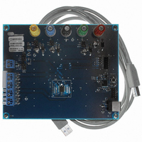
Manufacturer Part Number
CDB5532U
Description
BOARD EVAL FOR CS5532U ADC
Manufacturer
Cirrus Logic Inc
Specifications of CDB5532U
Number Of Adc's
2
Number Of Bits
24
Sampling Rate (per Second)
3.84k
Data Interface
Serial
Inputs Per Adc
1 Differential
Input Range
±2.5 V
Power (typ) @ Conditions
35mW @ 3.84kSPS
Voltage Supply Source
Analog and Digital, Dual ±
Operating Temperature
-40°C ~ 85°C
Utilized Ic / Part
CS5532
Description/function
Audio DSPs
Operating Supply Voltage
5 V
Product
Audio Modules
For Use With/related Products
C8051F320
Lead Free Status / RoHS Status
Contains lead / RoHS non-compliant
Lead Free Status / RoHS Status
Lead free / RoHS Compliant, Contains lead / RoHS non-compliant
Other names
598-1159


crocontroller and the ADC, and may prematurely
halt the calibration cycle.
For maximum accuracy, calibrations should be per-
formed for both offset and gain (selected by chang-
ing the G2-G0 bits of the channel-setup registers).
Note that only one gain range can be calibrated per
physical channel when the OGS bit in the Configu-
ration Register is set to ‘0’. Multiple gain ranges
can be calibrated for a single channel by manipulat-
ing the OGS bit and the OG1-OG0 bits of the se-
lected Setup (see Section 2.3.7 for more details). If
factory calibration of the user’s system is per-
formed using the system calibration capabilities of
the CS5532/34, the offset and gain register contents
can be read by the system microcontroller and re-
corded in non-volatile memory. These same cali-
bration words can then be uploaded into the offset
and gain registers of the converter when power is
first applied to the system, or when the gain range
is changed.
When the device is used without calibration, the
uncalibrated gain accuracy is about ±1% and the
gain tracking from range to range (2x to 64x) is ap-
proximately ±0.3 percent.
Note that the gain from the offset register to the
output is 1.83007966 decimal, not 1. If a user wants
to adjust the calibration coefficients externally,
they will need to divide the information to be writ-
ten to the offset register by the scale factor of
1.83007966. (This discussion assumes that the gain
register is 1.000...000 decimal. The offset register
is also multiplied by the gain register before being
applied to the output conversion words).
2.5.8. Limitations in Calibration Range
System calibration can be limited by signal head-
room in the analog signal path inside the chip as
discussed under the Analog Input section of this
data sheet. For gain calibration, the full-scale input
signal can be reduced to 3% of the nominal full-
scale value. At this point, the gain register is ap-
proximately equal to 33.33 (decimal). While the
DS755F3
gain register can hold numbers all the way up to 64
- 2
of 40 should not be used. With the converter’s in-
trinsic gain error, this minimum full-scale input
signal may be higher or lower. In defining the min-
imum Full Scale Calibration Range (FSCR) under
Analog Characteristics, margin is retained to ac-
commodate the intrinsic gain error. Inversely, the
input full-scale signal can be increased to a point in
which the modulator reaches its 1’s density limit of
86 percent, which under nominal conditions occurs
when the full-scale input signal is 1.1 times the
nominal full-scale value. With the chip’s intrinsic
gain error, this maximum full-scale input signal
maybe higher or lower. In defining the maximum
FSCR, margin is again incorporated to accommo-
date the intrinsic gain error.
2.6. Performing Conversions
The CS5532/34 offers two distinctly different con-
version modes. The three sections that follow detail
the differences and provide examples illustrating
how to use the conversion modes with the channel-
setup registers.
2.6.1. Single Conversion Mode
Based on the information provided in the channel-
setup registers (CSRs), after the user transmits the
conversion command, a single, fully settled con-
version is performed. The command byte includes
a pointer address to the Setup register to be used
during the conversion. Once transmitted, the serial
port enters data mode where it waits until the con-
version is complete. When the conversion data is
available, SDO falls to logic 0. Forty SCLKs are
then needed to read the conversion data word. The
first 8 SCLKs are used to clear the SDO flag. Dur-
ing the first 8 SCLKs, SDI must be logic 0. The last
32 SCLKs are needed to read the conversion result.
Note that the user is forced to read the conversion
in single conversion mode as SDO will remain low
(i.e. the serial port is in data mode) until SCLK
transitions 40 times. After reading the data, the se-
-24
, gain register settings above a decimal value
CS5532/34-BS
33
Related parts for CDB5532U
Image
Part Number
Description
Manufacturer
Datasheet
Request
R

Part Number:
Description:
Development Kit
Manufacturer:
Cirrus Logic Inc
Datasheet:
Part Number:
Description:
Development Kit
Manufacturer:
Cirrus Logic Inc
Datasheet:


Part Number:
Description:
High-efficiency PFC + Fluorescent Lamp Driver Reference Design
Manufacturer:
Cirrus Logic Inc
Datasheet:
Part Number:
Description:
Development Kit
Manufacturer:
Cirrus Logic Inc
Datasheet:
Part Number:
Description:
Development Kit
Manufacturer:
Cirrus Logic Inc
Datasheet:

Part Number:
Description:
Development Kit
Manufacturer:
Cirrus Logic Inc
Datasheet:
Part Number:
Description:
Development Kit
Manufacturer:
Cirrus Logic Inc
Datasheet:
Part Number:
Description:
Development Kit
Manufacturer:
Cirrus Logic Inc
Datasheet:
Part Number:
Description:
Development Kit
Manufacturer:
Cirrus Logic Inc
Datasheet:

Part Number:
Description:
EVALUATION BOARD FOR CS8427
Manufacturer:
Cirrus Logic Inc
Datasheet:

Part Number:
Description:
BOARD EVAL FOR CS8416 RCVR
Manufacturer:
Cirrus Logic Inc
Datasheet:

Part Number:
Description:
EVALUATION BOARD FOR CS8420
Manufacturer:
Cirrus Logic Inc
Datasheet:

Part Number:
Description:
KIT DEVELOPMENT EP9315 ARM9
Manufacturer:
Cirrus Logic Inc
Datasheet:

Part Number:
Description:
KIT DEVELOPMENT EP9302 ARM9
Manufacturer:
Cirrus Logic Inc
Datasheet: