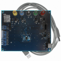
CDB5532U Cirrus Logic Inc, CDB5532U Datasheet - Page 31

CDB5532U
Manufacturer Part Number
CDB5532U
Description
BOARD EVAL FOR CS5532U ADC
Manufacturer
Cirrus Logic Inc
Specifications of CDB5532U
Number Of Adc's
2
Number Of Bits
24
Sampling Rate (per Second)
3.84k
Data Interface
Serial
Inputs Per Adc
1 Differential
Input Range
±2.5 V
Power (typ) @ Conditions
35mW @ 3.84kSPS
Voltage Supply Source
Analog and Digital, Dual ±
Operating Temperature
-40°C ~ 85°C
Utilized Ic / Part
CS5532
Description/function
Audio DSPs
Operating Supply Voltage
5 V
Product
Audio Modules
For Use With/related Products
C8051F320
Lead Free Status / RoHS Status
Contains lead / RoHS non-compliant
Lead Free Status / RoHS Status
Lead free / RoHS Compliant, Contains lead / RoHS non-compliant
Other names
598-1159
2.5.4. Performing Calibrations
To perform a calibration, the user must send a com-
mand byte with its MSB=1, its pointer bits
(CSRP2-CSRP0) set to address the desired Setup to
calibrate, and the appropriate calibration bits (CC2-
CC0) set to choose the type of calibration to be per-
formed. Note that calibration assumes that the
CSRs have been previously initialized because the
information concerning the physical channel, its
filter rate, gain range, and polarity, comes from the
channel-setup register addressed by the pointer bits
in the command byte. Once the CSRs are initial-
ized, a calibration can be performed with one com-
mand byte.
The length of time it takes to do a calibration is
slightly less than the amount of time it takes to do
a single conversion (see Table 1 for single conver-
sion timing). Offset calibration takes 608 clock cy-
cles less than a single conversion when FRS = 0,
and 729 clock cycles less when FRS = 1. Gain cal-
ibration takes 128 clock cycles less than a single
conversion when FRS = 0, and 153 clock cycles
less when FRS = 1.
Once a calibration cycle is complete, SDO falls and
the results are automatically stored in either the
gain or offset register for the physical channel be-
ing calibrated when the OGS bit in the Configura-
tion Register is set to ‘0’. If the OGS bit is set to ‘1’,
the results will be stored in the register specified by
the OG1-OG0 bits of the selected Setup. See the
OGS bit description for more details (Section
2.3.7). SDO will remain low until the next com-
mand word is begun. If additional calibrations are
performed while referencing the same calibration
DS755F3
registers, the last calibration results will replace the
effects from the previous calibration as only one
offset and gain register is available per physical
channel. Only one calibration is performed with
each command byte. To calibrate all the channels,
additional calibration commands are necessary.
2.5.5. Self Calibration
The CS5532/34 offer both self-offset and self-gain
calibrations. For the self calibration of offset, the
converters internally tie the inputs of the 1x ampli-
fier together and routes them to the AIN- pin as
shown in Figure 11. For accurate self calibration of
offset to occur, the AIN pins must be at the proper
common-mode voltage as specified in the Analog
Characteristics section. Self-offset calibration uses
the 1x gain amplifier, and is therefore not valid in the
2x-64x gain ranges. A self-offset calibration of these
gain ranges can be performed by setting the IS bit in
the configuration register to a ‘1’, and performing a
system offset calibration. The IS bit must be returned
to ‘0’ afterwards for normal operation of the device.
For self calibration of gain, the differential inputs
of the modulator are connected to VREF+ and
VREF- as shown in Figure 12. Self calibration of
gain will not work with (VREF+ - VREF-) > 2.5V.
Self calibration of gain is performed in the GAIN =
1x mode without regard to the setup register’s gain
setting. Gain errors in the PGIA gain steps 2x to
64x are not calibrated as this would require an ac-
curate low-voltage source other than the reference
voltage. A system calibration of gain should be per-
formed if accurate gains are to be achieved on the
ranges other than 1x, or when
(VREF+ – VREF-) > 2.5V.
CS5532/34-BS
31


