CDB5532U Cirrus Logic Inc, CDB5532U Datasheet - Page 24
CDB5532U
Manufacturer Part Number
CDB5532U
Description
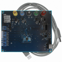
BOARD EVAL FOR CS5532U ADC
Manufacturer
Cirrus Logic Inc
Specifications of CDB5532U
Number Of Adc's
2
Number Of Bits
24
Sampling Rate (per Second)
3.84k
Data Interface
Serial
Inputs Per Adc
1 Differential
Input Range
±2.5 V
Power (typ) @ Conditions
35mW @ 3.84kSPS
Voltage Supply Source
Analog and Digital, Dual ±
Operating Temperature
-40°C ~ 85°C
Utilized Ic / Part
CS5532
Description/function
Audio DSPs
Operating Supply Voltage
5 V
Product
Audio Modules
For Use With/related Products
C8051F320
Lead Free Status / RoHS Status
Contains lead / RoHS non-compliant
Lead Free Status / RoHS Status
Lead free / RoHS Compliant, Contains lead / RoHS non-compliant
Other names
598-1159


ter is read. The on-chip registers are initialized to
the following default states:
After reset, the RS bit should be written back to
logic 0 to complete the reset cycle. The ADC will
return to the command mode where it waits for a
valid command. Also, the RS bit is the only bit in
the configuration register that can be set when ini-
tiating a reset (i.e. a second write command is need-
ed to set other bits in the Configuration Register
after the RS bit has been cleared).
2.3.3. Input Short
The input short bit allows the user to internally
ground all the inputs of the multiplexer. This is a
useful function because it allows the user to easily
test the grounded input performance of the ADC
and eliminate the noise effects due to the external
system components.
2.3.4. Guard Signal
The guard signal bit modifies the function of A0.
When set, this bit outputs the common mode volt-
age of the instrumentation amplifier on A0. This
feature is useful when the user wants to connect an
external shield to the common mode potential of
the instrumentation amplifier to protect against
leakage. Figure 8 illustrates a typical connection di-
agram for the guard signal.
2.3.5. Voltage Reference Select
The voltage reference select (VRS) bit selects the
size of the sampling capacitor used to sample the
voltage reference. The bit should be set based upon
the magnitude of the reference voltage to achieve
optimal performance. Figures 9 and 10 model the
effects on the reference’s input impedance and in-
put current for each VRS setting. As the models
show, the reference includes a coarse/fine charge
24
Configuration Register:
Offset Registers:
Gain Registers:
Channel Setup Registers: 00000000(H)
00000000(H)
00000000(H)
01000000(H)
buffer which reduces the dynamic current demand
of the external reference.
The reference’s input buffer is designed to accom-
modate rail-to-rail (common-mode plus signal) in-
put voltages. The differential voltage between the
VREF+ and VREF- can be any voltage from 1.0 V
up to the analog supply (depending on how VRS is
configured), however, the VREF+ cannot go above
VA+ and the VREF- pin can not go below VA-.
Note that the power supplies to the chip should be
established before the reference voltage.
2.3.6. Output Latch Pins
The A1-A0 pins of the ADCs mimic the D21-
D20/D5-D4 bits of the channel-setup registers if
the output latch select (OLS) bit is logic 0 (default).
If the OLS bit is logic 1, A1-A0 mimic the output
latch bit settings in the configuration register.
These two options give the user a choice of allow-
ing the latch outputs to change anytime a different
CSR is selected for a conversion, or to allow the
latch bits to remain latched to a fixed state (deter-
mined by the configuration register bit) for all CSR
selections. In either case, A1-A0 can be used to
control external multiplexers and other logic func-
tions outside the converter. The A1-A0 outputs can
sink or source at least 1 mA, but it is recommended
to limit drive currents to less than 20 µA to reduce
self-heating of the chip. These outputs are powered
C o m m o n M o d e = 2 .5 V
V
V
IN
IN
+
-
Figure 8. Guard Signal Shielding Scheme
A 0 /G U A R D
A IN +
A IN -
CS5532/34-BS
C S 5 5 3 1 /3 2 /3 3 /3 4
+ 5 V A +
c e n te r
o u t p
o u t m
DS755F3
x1
Related parts for CDB5532U
Image
Part Number
Description
Manufacturer
Datasheet
Request
R

Part Number:
Description:
Development Kit
Manufacturer:
Cirrus Logic Inc
Datasheet:
Part Number:
Description:
Development Kit
Manufacturer:
Cirrus Logic Inc
Datasheet:


Part Number:
Description:
High-efficiency PFC + Fluorescent Lamp Driver Reference Design
Manufacturer:
Cirrus Logic Inc
Datasheet:
Part Number:
Description:
Development Kit
Manufacturer:
Cirrus Logic Inc
Datasheet:
Part Number:
Description:
Development Kit
Manufacturer:
Cirrus Logic Inc
Datasheet:

Part Number:
Description:
Development Kit
Manufacturer:
Cirrus Logic Inc
Datasheet:
Part Number:
Description:
Development Kit
Manufacturer:
Cirrus Logic Inc
Datasheet:
Part Number:
Description:
Development Kit
Manufacturer:
Cirrus Logic Inc
Datasheet:
Part Number:
Description:
Development Kit
Manufacturer:
Cirrus Logic Inc
Datasheet:

Part Number:
Description:
EVALUATION BOARD FOR CS8427
Manufacturer:
Cirrus Logic Inc
Datasheet:

Part Number:
Description:
BOARD EVAL FOR CS8416 RCVR
Manufacturer:
Cirrus Logic Inc
Datasheet:

Part Number:
Description:
EVALUATION BOARD FOR CS8420
Manufacturer:
Cirrus Logic Inc
Datasheet:

Part Number:
Description:
KIT DEVELOPMENT EP9315 ARM9
Manufacturer:
Cirrus Logic Inc
Datasheet:

Part Number:
Description:
KIT DEVELOPMENT EP9302 ARM9
Manufacturer:
Cirrus Logic Inc
Datasheet: