NCP1606BOOSTGEVB ON Semiconductor, NCP1606BOOSTGEVB Datasheet - Page 11
NCP1606BOOSTGEVB
Manufacturer Part Number
NCP1606BOOSTGEVB
Description
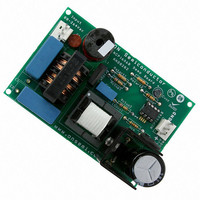
EVAL BOARD FOR NCP1606BOOSTG
Manufacturer
ON Semiconductor
Specifications of NCP1606BOOSTGEVB
Design Resources
NCP1606BOOST EVB BOM NCP1606BOOSTGEVB Gerber Files NCP1606BOOST EVB Schematic
Main Purpose
AC/DC, Primary and Secondary Side with PFC
Outputs And Type
1, Isolated
Power - Output
100W
Voltage - Output
400V
Current - Output
250mA
Voltage - Input
88 ~ 264VAC
Regulator Topology
Boost
Frequency - Switching
250kHz
Board Type
Fully Populated
Utilized Ic / Part
NCP1606
Lead Free Status / RoHS Status
Lead free / RoHS Compliant
For Use With/related Products
NCP1606BOOSTG
Other names
NCP1606BOOSTGEVBOS


linearly to its peak value. When the switch opens, the
inductor current linearly decreases to zero. At this point,
the drain voltage of the switch (V
and begins to drop. If the next switching cycle does not
start, then the voltage will ring with a dampened frequency
around V
in AND8123), leads to the result that good power factor
correction in CRM operation is achieved when the on time
is constant across an ac cycle and is equal to:
illustrated in Figure 24. The off time varies based on the
instantaneous line voltage, but the on time is kept constant.
This naturally causes the peak inductor current (I
follow the ac line voltage.
this constant on time CRM control in a cost effective and
robust solution. The device incorporates an accurate
regulation circuit, a low power startup circuit, and
advanced protection features.
EA sets the FB level. If the output voltage is too low, then
the FB level will drop and the EA will cause the control
voltage to increase. This increases the on time of the driver,
which increases the power delivered and brings the output
back into regulation. Alternatively, if the output voltage
(and hence FB voltage) is too high, then the control level
decreases and the driver on times are shortened. In this way,
the circuit regulates the output voltage (V
V
divider R
OUT
When the switch is closed, the inductor current increases
A simple plot of this switching over an ac line cycle is
The NCP1606 represents an ideal method to implement
A resistor divider from the boost output to the input of the
portion that is applied to FB through the resistor
in
OUT1
R
R
. A simple derivation of equations (such as found
OUT2
OUT1
V
OUT
and R
t on +
Control
OUT2
C
COMP
h @ Vac
2 @ P
FB
is equal to the internal reference
Figure 25. Error Amplifier and On Time Regulation Circuits
OUT
RMS
+
d
@ L
V
) is essentially floating
CONTROL
2
EA
2.5 V
+
−
OUT
) so that the
Lpk
http://onsemi.com
(eq. 1)
t
ON
) to
t
ON(max)
t
PWM
11
ERROR AMPLIFIER REGULATION
voltage based on its built in error amplifier (EA). The error
amplifier ’s negative terminal is pinned out to FB, the
positive terminal is tied to a 2.5 V ± 1.6% reference, and the
output is pinned out to Control (Figure 25).
(2.5 V). The output voltage can then be easily set according
to the following equation:
Control pins to reduce the speed at which the EA responds
to changes in the boost output. This is necessary due to the
nature of an active PFC circuit. The PFC stage absorbs a
sinusoidal current from a sinusoidal line voltage. Hence,
the converter provides the load with a power that matches
Figure 24. Inductor Waveform During CRM Operation
The NCP1606 is configured to regulate the boost output
A compensation network is placed between the FB and
MOSFET
Slope +
V
PWM BLOCK
EAL
V
I
OFF
I
ON
inpk
inpk
Lpk
I
CHARGE
V
OUT
Ct
V
CONTROL
+ 2.5 V @
R
OUT1
V
EAH
R
) R
OUT2
OUT2
V
in
(t)
I
L
(t)
I
in
(t)
(eq. 2)
Related parts for NCP1606BOOSTGEVB
Image
Part Number
Description
Manufacturer
Datasheet
Request
R

Part Number:
Description:
Cost Effective Power Factor Controller
Manufacturer:
ON Semiconductor
Datasheet:
Part Number:
Description:
ON Semiconductor [VOLTAGE REGULATOR]
Manufacturer:
ON Semiconductor
Datasheet:
Part Number:
Description:
357-036-542-201 CARDEDGE 36POS DL .156 BLK LOPRO
Manufacturer:
ON Semiconductor
Datasheet:
Part Number:
Description:
357-036-542-201 CARDEDGE 36POS DL .156 BLK LOPRO
Manufacturer:
ON Semiconductor
Datasheet:
Part Number:
Description:
357-036-542-201 CARDEDGE 36POS DL .156 BLK LOPRO
Manufacturer:
ON Semiconductor
Datasheet:
Part Number:
Description:
357-036-542-201 CARDEDGE 36POS DL .156 BLK LOPRO
Manufacturer:
ON Semiconductor
Datasheet:
Part Number:
Description:
357-036-542-201 CARDEDGE 36POS DL .156 BLK LOPRO
Manufacturer:
ON Semiconductor
Datasheet:
Part Number:
Description:
357-036-542-201 CARDEDGE 36POS DL .156 BLK LOPRO
Manufacturer:
ON Semiconductor
Datasheet:
Part Number:
Description:
357-036-542-201 CARDEDGE 36POS DL .156 BLK LOPRO
Manufacturer:
ON Semiconductor
Datasheet:
Part Number:
Description:
357-036-542-201 CARDEDGE 36POS DL .156 BLK LOPRO
Manufacturer:
ON Semiconductor
Datasheet:
Part Number:
Description:
357-036-542-201 CARDEDGE 36POS DL .156 BLK LOPRO
Manufacturer:
ON Semiconductor
Datasheet:
Part Number:
Description:
357-036-542-201 CARDEDGE 36POS DL .156 BLK LOPRO
Manufacturer:
ON Semiconductor
Datasheet:
Part Number:
Description:
Manufacturer:
ON Semiconductor
Datasheet:
Part Number:
Description:
Manufacturer:
ON Semiconductor
Datasheet: