NCP1606BOOSTGEVB ON Semiconductor, NCP1606BOOSTGEVB Datasheet - Page 4
NCP1606BOOSTGEVB
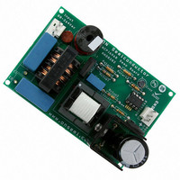
Manufacturer Part Number
NCP1606BOOSTGEVB
Description
EVAL BOARD FOR NCP1606BOOSTG
Manufacturer
ON Semiconductor
Specifications of NCP1606BOOSTGEVB
Design Resources
NCP1606BOOST EVB BOM NCP1606BOOSTGEVB Gerber Files NCP1606BOOST EVB Schematic
Main Purpose
AC/DC, Primary and Secondary Side with PFC
Outputs And Type
1, Isolated
Power - Output
100W
Voltage - Output
400V
Current - Output
250mA
Voltage - Input
88 ~ 264VAC
Regulator Topology
Boost
Frequency - Switching
250kHz
Board Type
Fully Populated
Utilized Ic / Part
NCP1606
Lead Free Status / RoHS Status
Lead free / RoHS Compliant
For Use With/related Products
NCP1606BOOSTG
Other names
NCP1606BOOSTGEVBOS


V
DEVICE CONSUMPTION
REGULATION BLOCK (ERROR AMPLIFIER)
CURRENT SENSE BLOCK
ZERO CURRENT DETECTION
3. Parameter values are valid for transient conditions only.
4. Parameter characterized and guaranteed by design, but not tested in production.
ELECTRICAL C
(Unless otherwise specified: For typical values, T
1 nF, Ct = 1 nF, CS = 0 V, Control = open, ZCD = open)
CC
I
V
V
CC(startup)
V
V
V
Symbol
I
I
V
V
REF
ZCD(HYS)
H
CC(fault)
CL(POS)
I
V
V
CL(POS)
UNDERVOLTAGE LOCKOUT SECTION
Control
V
EA
CS(limit)
V
V
CC(on)
CC(off)
I
I
I
G
t
BW
UVLO
ZCDH
ZCDL
CC1
CC2
I
I
t
I
ZCD
LEB
EAH
REF
EA
EAL
CS
CS
FB
OL
(diff)
(line)
V
V
Undervoltage Lockout Hysteresis
Icc consumption during startup: 0 V < V
Icc consumption after turn on at V
Icc consumption after turn on at V
Icc consumption after turn on at V
(such as during OVP fault, UVP fault, or grounding ZCD)
Voltage Reference
Vref Line Regulation from V
Error Amplifier Current Capability:: (Note 3)
Sink (Control = 4 V, V
Source (Control = 4 V, V
Open Loop, Error Amplifier Gain (Note 4)
Unity Gain Bandwidth (Note 4)
FB Bias Current @ V
Control Pin Bias Current @ FB = 0 V and Control = 4.0 V.
V
V
V
Overcurrent Protection Threshold:
NCP1606A
NCP1606B
Leading Edge Blanking duration
Overcurrent protection propagation delay.
CS bias current @ V
Zero Current Detection Threshold (V
Zero Current Detection Threshold (V
V
Maximum ZCD bias Current @ V
Upper Clamp Voltage @ I
Current Capability of the Positive Clamp at V
CC
CC
CONTROL
CONTROL
EA
ZCD
HARACTERISTICS
(diff) = V
Startup Threshold (Undervoltage Lockout Threshold, Vcc rising)
Disable Voltage after Turn On (Undervoltage Lockout Threshold, V
H − V
ZCD
@ I
@ I
EAH
EASOURCE
EASINK
L
− V
EAL
CS
FB
FB
= 0.5 mA, V
. Difference between max and min Control voltages
= 2 V
= 3 V
FB
= 2.6 V):
ZCD
= 0.5 mA, V
= 2.4 V):
CC(on)
= 2.5 mA
J
ZCD
CC
CC
CC
FB
+ 200 mV < V
= 25°C. For min/max values, T
ZCD
ZCD
= 12 V, No Load, 70 kHz switching
= 12 V, 1 nF Load, 70 kHz switching
= 12 V, 1 nF Load, no switching
= 2.6 V
= 5 V
FB
Rating
CC
= 2.4 V
rising)
falling)
http://onsemi.com
< V
ZCD
CC(on)
CC
= V
< 20 V, @ T
CL(POS)
− 200 mV
4
+ 200 mV:
−25°C < T
−40°C < T
−25°C < T
−40°C < T
−25°C < T
−40°C < T
J
= 25°C
J
= −40°C to +125°C, V
@ T
CC
J
J
J
J
J
J
< +125°C
< +125°C
< +125°C
< +125°C
< +125°C
< +125°C
falling)
J
= 25 °C
2.475
2.465
2.460
−500
10.9
1.85
0.45
1.45
11.0
Min
−20
150
300
8.7
8.5
2.2
8.0
4.9
3.0
1.6
1.9
5.0
CC
−2
−1
40
−1
−2
−
−
−
−
−
−
5
= 12 V, FB = 2.4 V, C
12.0
12.0
2.50
2.50
2.50
−6.0
Typ
250
100
500
9.5
9.5
2.5
1.4
2.1
1.2
5.3
2.1
3.2
1.7
0.5
2.1
1.6
5.7
8.5
20
17
80
−
1
−
−
−
−
2.525
2.535
2.540
Max
13.0
13.1
10.3
10.5
0.55
1.75
500
350
170
800
2.8
2.0
1.6
5.7
2.4
3.4
1.8
2.3
6.5
+2
40
30
−2
3
2
−
−
1
1
−
DRV
=
MHz
Unit
mA
mA
mA
mV
mA
mV
mA
mA
dB
nA
mA
mA
mA
ns
ns
V
V
V
V
V
V
V
V
V
V
V
Related parts for NCP1606BOOSTGEVB
Image
Part Number
Description
Manufacturer
Datasheet
Request
R

Part Number:
Description:
Cost Effective Power Factor Controller
Manufacturer:
ON Semiconductor
Datasheet:
Part Number:
Description:
ON Semiconductor [VOLTAGE REGULATOR]
Manufacturer:
ON Semiconductor
Datasheet:
Part Number:
Description:
357-036-542-201 CARDEDGE 36POS DL .156 BLK LOPRO
Manufacturer:
ON Semiconductor
Datasheet:
Part Number:
Description:
357-036-542-201 CARDEDGE 36POS DL .156 BLK LOPRO
Manufacturer:
ON Semiconductor
Datasheet:
Part Number:
Description:
357-036-542-201 CARDEDGE 36POS DL .156 BLK LOPRO
Manufacturer:
ON Semiconductor
Datasheet:
Part Number:
Description:
357-036-542-201 CARDEDGE 36POS DL .156 BLK LOPRO
Manufacturer:
ON Semiconductor
Datasheet:
Part Number:
Description:
357-036-542-201 CARDEDGE 36POS DL .156 BLK LOPRO
Manufacturer:
ON Semiconductor
Datasheet:
Part Number:
Description:
357-036-542-201 CARDEDGE 36POS DL .156 BLK LOPRO
Manufacturer:
ON Semiconductor
Datasheet:
Part Number:
Description:
357-036-542-201 CARDEDGE 36POS DL .156 BLK LOPRO
Manufacturer:
ON Semiconductor
Datasheet:
Part Number:
Description:
357-036-542-201 CARDEDGE 36POS DL .156 BLK LOPRO
Manufacturer:
ON Semiconductor
Datasheet:
Part Number:
Description:
357-036-542-201 CARDEDGE 36POS DL .156 BLK LOPRO
Manufacturer:
ON Semiconductor
Datasheet:
Part Number:
Description:
357-036-542-201 CARDEDGE 36POS DL .156 BLK LOPRO
Manufacturer:
ON Semiconductor
Datasheet:
Part Number:
Description:
Manufacturer:
ON Semiconductor
Datasheet:
Part Number:
Description:
Manufacturer:
ON Semiconductor
Datasheet: