NCP1606BOOSTGEVB ON Semiconductor, NCP1606BOOSTGEVB Datasheet - Page 2
NCP1606BOOSTGEVB
Manufacturer Part Number
NCP1606BOOSTGEVB
Description
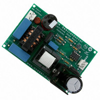
EVAL BOARD FOR NCP1606BOOSTG
Manufacturer
ON Semiconductor
Specifications of NCP1606BOOSTGEVB
Design Resources
NCP1606BOOST EVB BOM NCP1606BOOSTGEVB Gerber Files NCP1606BOOST EVB Schematic
Main Purpose
AC/DC, Primary and Secondary Side with PFC
Outputs And Type
1, Isolated
Power - Output
100W
Voltage - Output
400V
Current - Output
250mA
Voltage - Input
88 ~ 264VAC
Regulator Topology
Boost
Frequency - Switching
250kHz
Board Type
Fully Populated
Utilized Ic / Part
NCP1606
Lead Free Status / RoHS Status
Lead free / RoHS Compliant
For Use With/related Products
NCP1606BOOSTG
Other names
NCP1606BOOSTGEVBOS


AC IN
C
BULK
D
BOOST
L
BOOST
V
OUT
R
ZCD
C
R
R
R
COMP
SENSE
OUT1
OUT2
Control
Ct
ZCD
Ct
CS
FB
Shutdown
V
2.5 V
V
ESD
Clamp
ESD
ESD
ESD
CL(POS)
Active
Clamp
270 mA
CL(NEG)
V
nPOK
V
+
E/A
CONTROL
DD
+
300
mV
LEB
+
−
V
+
−
DD
+
+
Enable
+
200 mV
+
+
−
2.1 V
1.6 V
+
−
(Enable EA)
V
Figure 2. Block Diagram
+
−
Add V
CS(limit)
Offset
I
EAsink
Clamp
http://onsemi.com
OCP
+
V
−
Shutdown
V
Clamp
Measure
V
EAH
DD
Reset
UVP
EAL
EAL
*All values shown are typical only. Refer to the “Electrical Characteristics”
*All SR Latches are Reset Dominant
for complete specifications.
uV
Off Timer
Static OVP is triggered
when clamp is activated.
DD
DRV
2
Dynamic OVP
Static OVP
PWM
+
−
I
sink
S
R
Demag
Q
Q
>I
ovp
V
CC
ESD
nPOK
R
S
R
S
R
S
Q
Q
Q
Q
Q
Q
+
Fault
+
−
S
R
UVLO
Q
Q
POK
nPOK
V
UVLO
DD
V
V
Reg
ddGD
CC
uV
DD
V
V
DDGD
DD
V
CC
uV
DD
GND
DRV
Related parts for NCP1606BOOSTGEVB
Image
Part Number
Description
Manufacturer
Datasheet
Request
R

Part Number:
Description:
Cost Effective Power Factor Controller
Manufacturer:
ON Semiconductor
Datasheet:
Part Number:
Description:
ON Semiconductor [VOLTAGE REGULATOR]
Manufacturer:
ON Semiconductor
Datasheet:
Part Number:
Description:
357-036-542-201 CARDEDGE 36POS DL .156 BLK LOPRO
Manufacturer:
ON Semiconductor
Datasheet:
Part Number:
Description:
357-036-542-201 CARDEDGE 36POS DL .156 BLK LOPRO
Manufacturer:
ON Semiconductor
Datasheet:
Part Number:
Description:
357-036-542-201 CARDEDGE 36POS DL .156 BLK LOPRO
Manufacturer:
ON Semiconductor
Datasheet:
Part Number:
Description:
357-036-542-201 CARDEDGE 36POS DL .156 BLK LOPRO
Manufacturer:
ON Semiconductor
Datasheet:
Part Number:
Description:
357-036-542-201 CARDEDGE 36POS DL .156 BLK LOPRO
Manufacturer:
ON Semiconductor
Datasheet:
Part Number:
Description:
357-036-542-201 CARDEDGE 36POS DL .156 BLK LOPRO
Manufacturer:
ON Semiconductor
Datasheet:
Part Number:
Description:
357-036-542-201 CARDEDGE 36POS DL .156 BLK LOPRO
Manufacturer:
ON Semiconductor
Datasheet:
Part Number:
Description:
357-036-542-201 CARDEDGE 36POS DL .156 BLK LOPRO
Manufacturer:
ON Semiconductor
Datasheet:
Part Number:
Description:
357-036-542-201 CARDEDGE 36POS DL .156 BLK LOPRO
Manufacturer:
ON Semiconductor
Datasheet:
Part Number:
Description:
357-036-542-201 CARDEDGE 36POS DL .156 BLK LOPRO
Manufacturer:
ON Semiconductor
Datasheet:
Part Number:
Description:
Manufacturer:
ON Semiconductor
Datasheet:
Part Number:
Description:
Manufacturer:
ON Semiconductor
Datasheet: