NCP1606BOOSTGEVB ON Semiconductor, NCP1606BOOSTGEVB Datasheet - Page 14
NCP1606BOOSTGEVB
Manufacturer Part Number
NCP1606BOOSTGEVB
Description
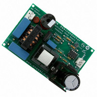
EVAL BOARD FOR NCP1606BOOSTG
Manufacturer
ON Semiconductor
Specifications of NCP1606BOOSTGEVB
Design Resources
NCP1606BOOST EVB BOM NCP1606BOOSTGEVB Gerber Files NCP1606BOOST EVB Schematic
Main Purpose
AC/DC, Primary and Secondary Side with PFC
Outputs And Type
1, Isolated
Power - Output
100W
Voltage - Output
400V
Current - Output
250mA
Voltage - Input
88 ~ 264VAC
Regulator Topology
Boost
Frequency - Switching
250kHz
Board Type
Fully Populated
Utilized Ic / Part
NCP1606
Lead Free Status / RoHS Status
Lead free / RoHS Compliant
For Use With/related Products
NCP1606BOOSTG
Other names
NCP1606BOOSTGEVBOS


internally clamped to V
ZCD winding is negative. Similarly, the ZCD pin is
clamped to V
too high. Because of these clamps, a resistor (R
Figure 29) is necessary to limit the current from the ZCD
winding to the ZCD pin.
therefore no voltage signal to activate the ZCD
comparators. This means that the driver could never turn
on. Therefore, to enable the PFC stage to startup under
these conditions, an internal watchdog timer is integrated
into the controller. This timer turns the drive on if the driver
has been off for more than 180 ms (typical). Obviously, this
feature is deactivated during a fault mode (OVP, UVP, or
Shutdown), and reactivated when the fault is removed.
STARTUP
V
(12 V typical). Because of the very low consumption of the
NCP1606 during this stage (< 40 mA), most of the current
goes directly to charging up the V
provides faster startup times and reduced standby power
dissipation. When the V
QUICK START and SOFT START
pulled up to V
of control voltage which produces output drives. This
feature, called “quick start,” eliminates the delay at startup
CC
To prevent negative voltages on the ZCD pin, the pin is
At startup, there is no energy in the ZCD winding and
Generally, a resistor connected between the ac input and
At startup, the error amplifier is enabled and Control is
(pin 8) charges the V
1
2
3
4
CL(POS)
EAL
(typically 2.1 V). This is the lowest level
(5.7 V typical), when the voltage rises
Figure 31. NCP1606 Supplied by a Downstream SMPS Controller (NCP1230)
8
7
6
5
CL(NEG)
CC
CC
+
PFC_Vcc
capacitor to the V
voltage exceeds the V
(600 mV typ) when the
CC
1
2
3
4
NCP1230
capacitor. This
D
boost
CC(on)
8
7
6
5
ZCD
http://onsemi.com
CC(on)
V
level
CC
+
in
+
14
C
level, the internal references and logic of the NCP1606 turn
on. The controller has an undervoltage lockout (UVLO)
feature which keeps the part active until V
V
for the auxiliary winding to take over and supply the
necessary power to V
power supply (SMPS), then it is often preferable to have the
SMPS controller startup first. The SMPS can then supply
the NCP1606 V
the NCP1230 or NCP1381, can control when to turn on the
PFC stage (see Figure 31) leading to optimal system
performance. This setup also eliminates the startup
resistors and therefore improves the no load power
dissipation of the system.
associated with charging the compensation network to its
minimum level. This also produces a natural “soft start”
mode where the controller’s power ramps up from zero to
the required power (see Figure 32).
bulk
V
CC(off)
When the PFC pre−converter is loaded by a switch mode
CC
Figure 30. Typical V
(9.5 V typical). This hysteresis allows ample time
CC
directly. Advanced controllers, such as
+
CC
V
V
CC(on)
CC(off)
(Figure 30).
CC
Startup Waveform
+
CC
drops below
Related parts for NCP1606BOOSTGEVB
Image
Part Number
Description
Manufacturer
Datasheet
Request
R

Part Number:
Description:
Cost Effective Power Factor Controller
Manufacturer:
ON Semiconductor
Datasheet:
Part Number:
Description:
ON Semiconductor [VOLTAGE REGULATOR]
Manufacturer:
ON Semiconductor
Datasheet:
Part Number:
Description:
357-036-542-201 CARDEDGE 36POS DL .156 BLK LOPRO
Manufacturer:
ON Semiconductor
Datasheet:
Part Number:
Description:
357-036-542-201 CARDEDGE 36POS DL .156 BLK LOPRO
Manufacturer:
ON Semiconductor
Datasheet:
Part Number:
Description:
357-036-542-201 CARDEDGE 36POS DL .156 BLK LOPRO
Manufacturer:
ON Semiconductor
Datasheet:
Part Number:
Description:
357-036-542-201 CARDEDGE 36POS DL .156 BLK LOPRO
Manufacturer:
ON Semiconductor
Datasheet:
Part Number:
Description:
357-036-542-201 CARDEDGE 36POS DL .156 BLK LOPRO
Manufacturer:
ON Semiconductor
Datasheet:
Part Number:
Description:
357-036-542-201 CARDEDGE 36POS DL .156 BLK LOPRO
Manufacturer:
ON Semiconductor
Datasheet:
Part Number:
Description:
357-036-542-201 CARDEDGE 36POS DL .156 BLK LOPRO
Manufacturer:
ON Semiconductor
Datasheet:
Part Number:
Description:
357-036-542-201 CARDEDGE 36POS DL .156 BLK LOPRO
Manufacturer:
ON Semiconductor
Datasheet:
Part Number:
Description:
357-036-542-201 CARDEDGE 36POS DL .156 BLK LOPRO
Manufacturer:
ON Semiconductor
Datasheet:
Part Number:
Description:
357-036-542-201 CARDEDGE 36POS DL .156 BLK LOPRO
Manufacturer:
ON Semiconductor
Datasheet:
Part Number:
Description:
Manufacturer:
ON Semiconductor
Datasheet:
Part Number:
Description:
Manufacturer:
ON Semiconductor
Datasheet: