NCP1606BOOSTGEVB ON Semiconductor, NCP1606BOOSTGEVB Datasheet - Page 15
NCP1606BOOSTGEVB
Manufacturer Part Number
NCP1606BOOSTGEVB
Description
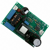
EVAL BOARD FOR NCP1606BOOSTG
Manufacturer
ON Semiconductor
Specifications of NCP1606BOOSTGEVB
Design Resources
NCP1606BOOST EVB BOM NCP1606BOOSTGEVB Gerber Files NCP1606BOOST EVB Schematic
Main Purpose
AC/DC, Primary and Secondary Side with PFC
Outputs And Type
1, Isolated
Power - Output
100W
Voltage - Output
400V
Current - Output
250mA
Voltage - Input
88 ~ 264VAC
Regulator Topology
Boost
Frequency - Switching
250kHz
Board Type
Fully Populated
Utilized Ic / Part
NCP1606
Lead Free Status / RoHS Status
Lead free / RoHS Compliant
For Use With/related Products
NCP1606BOOSTG
Other names
NCP1606BOOSTGEVBOS


Overvoltage Protection
active PFC stages very slow systems. One consequence of
this is the risk of huge overshoots in abrupt transient phases
(startup, load steps, etc.). For reliable operation, it is
critical that some form of overvoltage protection (OVP)
effectively prevents the output voltage from rising too
high. The NCP1606 detects these excessive V
FB
Control
V
V
CC
OUT
I
The low bandwidth of the feedback network makes
switch
2.5 V
V
Figure 32. Startup Timing Diagram Showing the
EAL
Natural Soft Start of the Control Pin
Natural Soft Start
V
V
+
CC(on)
CC(off)
+
−
UVLO
Figure 33. Output Driver Stage and Pull Down Clamps
V
DD REG
OUT
http://onsemi.com
V
V
levels
DD
ddGD
V
CC
DRV IN
15
UVLO
uV
DD
OUTPUT DRIVER
of peak currents of +500 mA and −800 mA. This enables
the controller to efficiently drive power MOSFETs for
medium power (up to 300 W) applications. Additionally,
the driver stage is equipped with both passive and active
pull down clamps (Figure 33). The clamps are active when
V
threshold voltage of a power MOSFET.
and disables the driver until the output voltage returns to
nominal levels. This keeps the output voltage within an
acceptable range. The limit is adjustable so that the
overvoltage level can be optimally set. The level must not
be so low that it is triggered by the 100 or 120 Hz ripple of
the output voltage. But it must be low enough so as not to
require a larger voltage rating of the output capacitor.
Figure 34 depicts the operation of the OVP circuitry.
CC
The NCP1606 includes a powerful output driver capable
is off and force the driver output to well below the
GND
DRV
Related parts for NCP1606BOOSTGEVB
Image
Part Number
Description
Manufacturer
Datasheet
Request
R

Part Number:
Description:
Cost Effective Power Factor Controller
Manufacturer:
ON Semiconductor
Datasheet:
Part Number:
Description:
ON Semiconductor [VOLTAGE REGULATOR]
Manufacturer:
ON Semiconductor
Datasheet:
Part Number:
Description:
357-036-542-201 CARDEDGE 36POS DL .156 BLK LOPRO
Manufacturer:
ON Semiconductor
Datasheet:
Part Number:
Description:
357-036-542-201 CARDEDGE 36POS DL .156 BLK LOPRO
Manufacturer:
ON Semiconductor
Datasheet:
Part Number:
Description:
357-036-542-201 CARDEDGE 36POS DL .156 BLK LOPRO
Manufacturer:
ON Semiconductor
Datasheet:
Part Number:
Description:
357-036-542-201 CARDEDGE 36POS DL .156 BLK LOPRO
Manufacturer:
ON Semiconductor
Datasheet:
Part Number:
Description:
357-036-542-201 CARDEDGE 36POS DL .156 BLK LOPRO
Manufacturer:
ON Semiconductor
Datasheet:
Part Number:
Description:
357-036-542-201 CARDEDGE 36POS DL .156 BLK LOPRO
Manufacturer:
ON Semiconductor
Datasheet:
Part Number:
Description:
357-036-542-201 CARDEDGE 36POS DL .156 BLK LOPRO
Manufacturer:
ON Semiconductor
Datasheet:
Part Number:
Description:
357-036-542-201 CARDEDGE 36POS DL .156 BLK LOPRO
Manufacturer:
ON Semiconductor
Datasheet:
Part Number:
Description:
357-036-542-201 CARDEDGE 36POS DL .156 BLK LOPRO
Manufacturer:
ON Semiconductor
Datasheet:
Part Number:
Description:
357-036-542-201 CARDEDGE 36POS DL .156 BLK LOPRO
Manufacturer:
ON Semiconductor
Datasheet:
Part Number:
Description:
Manufacturer:
ON Semiconductor
Datasheet:
Part Number:
Description:
Manufacturer:
ON Semiconductor
Datasheet: