NCP1606BOOSTGEVB ON Semiconductor, NCP1606BOOSTGEVB Datasheet - Page 9
NCP1606BOOSTGEVB
Manufacturer Part Number
NCP1606BOOSTGEVB
Description
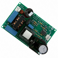
EVAL BOARD FOR NCP1606BOOSTG
Manufacturer
ON Semiconductor
Specifications of NCP1606BOOSTGEVB
Design Resources
NCP1606BOOST EVB BOM NCP1606BOOSTGEVB Gerber Files NCP1606BOOST EVB Schematic
Main Purpose
AC/DC, Primary and Secondary Side with PFC
Outputs And Type
1, Isolated
Power - Output
100W
Voltage - Output
400V
Current - Output
250mA
Voltage - Input
88 ~ 264VAC
Regulator Topology
Boost
Frequency - Switching
250kHz
Board Type
Fully Populated
Utilized Ic / Part
NCP1606
Lead Free Status / RoHS Status
Lead free / RoHS Compliant
For Use With/related Products
NCP1606BOOSTG
Other names
NCP1606BOOSTGEVBOS


Introduction
(PFC) controller designed to drive cost effective
pre−converters to meet input line harmonic regulations.
This controller operates in critical conduction mode
(CRM) for optimal performance in applications up to about
300 W. Its voltage mode scheme enables it to obtain unity
power factor without the need for a line sensing network.
The output voltage is accurately controlled by a high
precision error amplifier. The controller also implements a
comprehensive array of safety features for robust designs.
The key features of the NCP1606 are as follows:
•
•
•
•
•
•
•
•
The NCP1606 is a voltage mode power factor correction
Constant on time (Voltage Mode) CRM operation.
High power factor ratios are easily obtained without
the need for input voltage sensing. This allows for
optimal standby power consumption.
Accurate and Programmable On Time Limitation. The
NCP1606 using an accurate current source and an
external capacitor to generate the on time.
High Precision Voltage Reference. The error amplifier
reference voltage is guaranteed at 2.5 V ±1.6% over
process and temperature. This results in very accurate
output voltages.
Very Low Startup Consumption. The circuit
consumption is reduced to a minimum (< 40 mA)
during the startup phase which allows fast, low loss,
charging of V
gives a controlled undervoltage lockout level and
provides ample V
Powerful Output Driver. A −500 mA / +800 mA totem
pole gate driver is used to provide rapid turn on and
turn off times. This translates into improved
efficiencies and the ability to drive higher power
MOSFETs. Additionally, a combination of active and
passive circuitry is used to ensure that the driver
output voltage does not float high while V
its turn on level.
Programmable Overvoltage Protection (OVP). The
adjustable OVP feature protects the PFC stage against
excessive output overshoots that could damage the
application. These events can typically occur during
the startup phase or when the load is abruptly
removed. The NCP1606B gives a lower OVP
threshold, which can further reduce the application’s
standby power loss.
Protection against Open Loop (Undervoltage
Protection). Undervoltage protection (UVP) disables
the PFC stage when the output voltage is excessively
low. This also protects the circuit in case of a failure in
the feedback network: if no voltage is applied to FB
because of a bad connection, UVP is activated and
shuts down the pre−converter.
Overcurrent Limitation. The peak current is accurately
limited on a pulse by pulse basis. The level is
adjustable by modifying the switch sense resistor. The
CC
. The architecture of the NCP1606
CC
hysteresis during startup.
CC
is below
http://onsemi.com
9
•
Application information
use a diode bridge rectifier and a bulk storage capacitor to
produce a dc voltage from the utility ac line (Figure 20).
This DC voltage is then processed by additional circuitry
to drive the desired output.
when the instantaneous ac voltage exceeds the capacitor
voltage. Since this occurs near the line voltage peak, the
resulting current draw is non sinusoidal and contains a very
high harmonic content. This results in a poor power factor
(typically < 0.6) and consequently, the apparent input
power is much higher than the real power delivered to the
load. Additionally, if multiple devices are tied to the same
input line, the effect is magnified and a “line sag” effect can
be produced (see Figure 21).
requirements necessitate control over the line current
harmonic content. To meet this need, power factor
correction is implemented with either a passive or active
circuit. Passive circuits usually contain a combination of
large capacitors, inductors, and rectifiers that operate at the
ac line frequency. Active circuits incorporate some form of
AC Line Current
Most electronic ballasts and switching power supplies
This simple rectifying circuit draws power from the line
Increasingly,
NCP1606B uses a lower overcurrent threshold, which
can further reduce the application’s power dissipation.
An integrated LEB filter reduces the chance of noise
prematurely triggering the overcurrent limit.
Shutdown Features. The PFC pre−converter can be
easily placed in a shutdown mode by grounding either
the FB pin or the ZCD pin. During this mode, the I
current consumption is reduced and the error amplifier
is disabled.
AC Line Voltage
Figure 21. Typical Line Waveforms without PFC
Line
Rectified DC
AC
Figure 20. Typical Circuit without PFC
V
pk
0
0
Rectifiers
government
+
Line
Sag
Capacitor
Bulk
Storage
regulations
Converter
and
utility
Load
CC
Related parts for NCP1606BOOSTGEVB
Image
Part Number
Description
Manufacturer
Datasheet
Request
R

Part Number:
Description:
Cost Effective Power Factor Controller
Manufacturer:
ON Semiconductor
Datasheet:
Part Number:
Description:
ON Semiconductor [VOLTAGE REGULATOR]
Manufacturer:
ON Semiconductor
Datasheet:
Part Number:
Description:
357-036-542-201 CARDEDGE 36POS DL .156 BLK LOPRO
Manufacturer:
ON Semiconductor
Datasheet:
Part Number:
Description:
357-036-542-201 CARDEDGE 36POS DL .156 BLK LOPRO
Manufacturer:
ON Semiconductor
Datasheet:
Part Number:
Description:
357-036-542-201 CARDEDGE 36POS DL .156 BLK LOPRO
Manufacturer:
ON Semiconductor
Datasheet:
Part Number:
Description:
357-036-542-201 CARDEDGE 36POS DL .156 BLK LOPRO
Manufacturer:
ON Semiconductor
Datasheet:
Part Number:
Description:
357-036-542-201 CARDEDGE 36POS DL .156 BLK LOPRO
Manufacturer:
ON Semiconductor
Datasheet:
Part Number:
Description:
357-036-542-201 CARDEDGE 36POS DL .156 BLK LOPRO
Manufacturer:
ON Semiconductor
Datasheet:
Part Number:
Description:
357-036-542-201 CARDEDGE 36POS DL .156 BLK LOPRO
Manufacturer:
ON Semiconductor
Datasheet:
Part Number:
Description:
357-036-542-201 CARDEDGE 36POS DL .156 BLK LOPRO
Manufacturer:
ON Semiconductor
Datasheet:
Part Number:
Description:
357-036-542-201 CARDEDGE 36POS DL .156 BLK LOPRO
Manufacturer:
ON Semiconductor
Datasheet:
Part Number:
Description:
357-036-542-201 CARDEDGE 36POS DL .156 BLK LOPRO
Manufacturer:
ON Semiconductor
Datasheet:
Part Number:
Description:
Manufacturer:
ON Semiconductor
Datasheet:
Part Number:
Description:
Manufacturer:
ON Semiconductor
Datasheet: