NCP1606BOOSTGEVB ON Semiconductor, NCP1606BOOSTGEVB Datasheet - Page 13
NCP1606BOOSTGEVB
Manufacturer Part Number
NCP1606BOOSTGEVB
Description
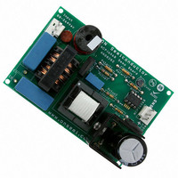
EVAL BOARD FOR NCP1606BOOSTG
Manufacturer
ON Semiconductor
Specifications of NCP1606BOOSTGEVB
Design Resources
NCP1606BOOST EVB BOM NCP1606BOOSTGEVB Gerber Files NCP1606BOOST EVB Schematic
Main Purpose
AC/DC, Primary and Secondary Side with PFC
Outputs And Type
1, Isolated
Power - Output
100W
Voltage - Output
400V
Current - Output
250mA
Voltage - Input
88 ~ 264VAC
Regulator Topology
Boost
Frequency - Switching
250kHz
Board Type
Fully Populated
Utilized Ic / Part
NCP1606
Lead Free Status / RoHS Status
Lead free / RoHS Compliant
For Use With/related Products
NCP1606BOOSTG
Other names
NCP1606BOOSTGEVBOS


out the bulk voltage ripple, then this on time is truly
constant over the ac line cycle.
when V
capacitor must be sized to ensure that the required on time
can be delivered at full power and the lowest input voltage
condition. The maximum on time is given by:
OFF TIME SEQUENCE
time in CRM operation varies with the instantaneous input
voltage. The NCP1606 determines the correct off time by
sensing the inductor voltage. When the inductor current
drops to zero, the drain voltage (“Vd” in Figure 23) is
essentially floating and naturally begins to drop. If the
switch is turned on at this moment, then CRM operation
will be achieved. To measure this high voltage directly on
the inductor is generally not economical or practical.
Rather, a smaller winding is taken off of the boost inductor.
This winding, called the zero current detector (ZCD)
winding, gives a scaled version of the inductor output and
is more useful to the controller.
Note that the maximum on time of the controller occurs
Combining this equation with equation 1, gives:
where V
I
While the on time is constant across the ac cycle, the off
V
CHARGE
in
CONTROL
CTMAX
= 297 mA (max)
N
N
Ct w
ZCD
B
t
ON(max)
R
= 2.9 V (min)
is at its maximum. Therefore, the Ct
ZCD
2 @ P
h @ Vac
OUT
+
R
RMS
Ct @ V
SENSE
@ L @ I
I
CHARGE
2
ZCD
@ V
CTMAX
CHARGE
Figure 29. Implementation of the ZCD Winding
CTMAX
VCL(NEG)
VCL(POS)
Active
Clamp
Clamp
V
DD
http://onsemi.com
(eq. 4)
(eq. 5)
+
200 mV
13
+
+
−
+
ZCD winding. When the drive is on, a negative voltage
appears on the ZCD winding. And when the drive is off, a
positive voltage appears. When the inductor current drops
to zero, then the ZCD voltage falls and starts to ring around
zero volts. The NCP1606 detects this falling edge and starts
the next driver on time. To ensure that a ZCD event has
truly occurred, the NCP1606’s logic (Figure 29) waits for
the ZCD pin voltage to rise above V
and then fall below V
CRM operation is easily achieved.
DRIVE
Drain
ZCD
Winding
Pin
Figure 28 gives typical operating waveforms with the
2.1 v
1.6 V
Figure 28. Voltage Waveforms for Zero Current
+
−
+
−
V
5.7 V
2.1 V
1.6 V
0.6 V
OUT
Shutdown
DRIVE
ZCDL
Detection
(1.6 V typical). In this way,
Dominant
R
S
Latch
Reset
ZCDH
Q
Q
Demag
(2.1 V typical)
Related parts for NCP1606BOOSTGEVB
Image
Part Number
Description
Manufacturer
Datasheet
Request
R

Part Number:
Description:
Cost Effective Power Factor Controller
Manufacturer:
ON Semiconductor
Datasheet:
Part Number:
Description:
ON Semiconductor [VOLTAGE REGULATOR]
Manufacturer:
ON Semiconductor
Datasheet:
Part Number:
Description:
357-036-542-201 CARDEDGE 36POS DL .156 BLK LOPRO
Manufacturer:
ON Semiconductor
Datasheet:
Part Number:
Description:
357-036-542-201 CARDEDGE 36POS DL .156 BLK LOPRO
Manufacturer:
ON Semiconductor
Datasheet:
Part Number:
Description:
357-036-542-201 CARDEDGE 36POS DL .156 BLK LOPRO
Manufacturer:
ON Semiconductor
Datasheet:
Part Number:
Description:
357-036-542-201 CARDEDGE 36POS DL .156 BLK LOPRO
Manufacturer:
ON Semiconductor
Datasheet:
Part Number:
Description:
357-036-542-201 CARDEDGE 36POS DL .156 BLK LOPRO
Manufacturer:
ON Semiconductor
Datasheet:
Part Number:
Description:
357-036-542-201 CARDEDGE 36POS DL .156 BLK LOPRO
Manufacturer:
ON Semiconductor
Datasheet:
Part Number:
Description:
357-036-542-201 CARDEDGE 36POS DL .156 BLK LOPRO
Manufacturer:
ON Semiconductor
Datasheet:
Part Number:
Description:
357-036-542-201 CARDEDGE 36POS DL .156 BLK LOPRO
Manufacturer:
ON Semiconductor
Datasheet:
Part Number:
Description:
357-036-542-201 CARDEDGE 36POS DL .156 BLK LOPRO
Manufacturer:
ON Semiconductor
Datasheet:
Part Number:
Description:
357-036-542-201 CARDEDGE 36POS DL .156 BLK LOPRO
Manufacturer:
ON Semiconductor
Datasheet:
Part Number:
Description:
Manufacturer:
ON Semiconductor
Datasheet:
Part Number:
Description:
Manufacturer:
ON Semiconductor
Datasheet: