NCP1606BOOSTGEVB ON Semiconductor, NCP1606BOOSTGEVB Datasheet - Page 19
NCP1606BOOSTGEVB
Manufacturer Part Number
NCP1606BOOSTGEVB
Description
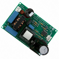
EVAL BOARD FOR NCP1606BOOSTG
Manufacturer
ON Semiconductor
Specifications of NCP1606BOOSTGEVB
Design Resources
NCP1606BOOST EVB BOM NCP1606BOOSTGEVB Gerber Files NCP1606BOOST EVB Schematic
Main Purpose
AC/DC, Primary and Secondary Side with PFC
Outputs And Type
1, Isolated
Power - Output
100W
Voltage - Output
400V
Current - Output
250mA
Voltage - Input
88 ~ 264VAC
Regulator Topology
Boost
Frequency - Switching
250kHz
Board Type
Fully Populated
Utilized Ic / Part
NCP1606
Lead Free Status / RoHS Status
Lead free / RoHS Compliant
For Use With/related Products
NCP1606BOOSTG
Other names
NCP1606BOOSTGEVBOS


BOOST DESIGN EQUATIONS
RMS Input Current
Maximum Inductor Peak
Current
Inductor Value
Maximum On Time
Off Time
Frequency
Pin 3 Capacitor
Boost Turns to ZCD Turns
Ratio
Resistor from ZCD wind-
ing to the ZCD pin (pin 5)
Boost Output Voltage
Maximum V
prior to OVP activation and
the necessary R
R
Minimum output voltage
necessary to exit under-
voltage protection (UVP)
Bulk Cap Ripple
Inductor RMS Current
Boost Diode RMS Current
MOSFET RMS Current
OUT2
.
OUT
voltage
OUT1
and
f
SW
Components are identified in Figure 1
Id
I
M(rms)
+
MAX(rms)
Vripple
V
Vac
2 @ L @ P
OUT(max)
V
V
L v
OUT
N
R
OUT(nom)
+ 2
R
B
OUT1
(rms)
R
Ct w
(pk−pk)
ZCD
: N
V
(UVP)
Icoil
+ 4
OUT2
t
t
I
OFF
ON(max)
pk(max)
3
OUT
I
2
ac(rms)
ZCD
OUT
2 @ Vac
3
@ Pin
+
+ V
w
@ h
RMS
2 @ P
+
h @ Vac
@
Vac
+
+ 2.5 V @
+
@ Vac @ I
+
V
I
v
CL(NEG)
@
http://onsemi.com
R
OUT(max)
OUT(nom)
Vac (rms) @ sin(q) @ 2
+
C
V
+
+
2 @ 2
OUT1
+
@
OUT
V
OUT(nom)
bulk
2
2.5 V @ R
1 *
2 @ 2 @ P
OUT
p
@
2 @ L @ P
Vac
h @ V
RMS
R
3 @ Vac
h @ Vac
V
h @ Vac
OUT
@ L @ I
@ 2 @ p @ f
2 @ P
OUT2
pk(max)
) R
V
t
@ (N
1 *
P
I
@
ON
Vac
* Vac
OUT
HL
R
19
V
OVP
2
* V
OUT
) R
2
ac(rms)
h @ Vac
OUT1
@ V
ZCDH
P
@ 2
* 2.5 V
OUT2
B
OUT
* Vac
(rms)
OUT
CHARGE
OUT1
LL
LL
OUT
R
LL
: N
OUT(nom)
8 @ 2 @ Vac
OUT
@ f
CTMAX
OUT1
3 p @ V
* 1
HL
OUT2
2
@ h
) R
V
line
SW(min)
ZCD
P
@ V
@ | sin q | @ 2
OUT
@ 2
OUT
LL
@ I
@ V
OUT2
)
UVP
@ V
OUT
OVP
OUT
OUT
h (the efficiency of only the Boost
PFC stage) is generally in the range
of 90 − 95%
I
voltage.
f
switching frequency. The maximum L
must be calculated at low line and
high line.
The maximum on time occurs at the
lowest line voltage and maximum
output power.
The off time is greatest at the peak of
the AC line voltage and approaches
zero at the AC line zero crossings.
Theta (q) represents the angle of the
AC line voltage.
I
the NCP1606 specification table.
The turns ratio must be low enough
so as to trigger the ZCD comparators
at high line.
R
the shutdown comparator is not inad-
vertently activated.
I
cification table. I
NCP1606B, then for the NCP1606A
version.
V
cification table.
Use f
universal lines. The ripple must not
exceed the OVP level for V
pk(max)
SW(min)
CHARGE
OVP
UVP
ZCD
is given in the NCP1606 spe-
line
must be large enough so that
is given in the NCP1606 spe-
occurs at the lowest line
is the minimum desired
= 47 Hz for worst case at
and V
CTMAX
OVP
is lower for the
are given in
OUT
.
Related parts for NCP1606BOOSTGEVB
Image
Part Number
Description
Manufacturer
Datasheet
Request
R

Part Number:
Description:
Cost Effective Power Factor Controller
Manufacturer:
ON Semiconductor
Datasheet:
Part Number:
Description:
ON Semiconductor [VOLTAGE REGULATOR]
Manufacturer:
ON Semiconductor
Datasheet:
Part Number:
Description:
357-036-542-201 CARDEDGE 36POS DL .156 BLK LOPRO
Manufacturer:
ON Semiconductor
Datasheet:
Part Number:
Description:
357-036-542-201 CARDEDGE 36POS DL .156 BLK LOPRO
Manufacturer:
ON Semiconductor
Datasheet:
Part Number:
Description:
357-036-542-201 CARDEDGE 36POS DL .156 BLK LOPRO
Manufacturer:
ON Semiconductor
Datasheet:
Part Number:
Description:
357-036-542-201 CARDEDGE 36POS DL .156 BLK LOPRO
Manufacturer:
ON Semiconductor
Datasheet:
Part Number:
Description:
357-036-542-201 CARDEDGE 36POS DL .156 BLK LOPRO
Manufacturer:
ON Semiconductor
Datasheet:
Part Number:
Description:
357-036-542-201 CARDEDGE 36POS DL .156 BLK LOPRO
Manufacturer:
ON Semiconductor
Datasheet:
Part Number:
Description:
357-036-542-201 CARDEDGE 36POS DL .156 BLK LOPRO
Manufacturer:
ON Semiconductor
Datasheet:
Part Number:
Description:
357-036-542-201 CARDEDGE 36POS DL .156 BLK LOPRO
Manufacturer:
ON Semiconductor
Datasheet:
Part Number:
Description:
357-036-542-201 CARDEDGE 36POS DL .156 BLK LOPRO
Manufacturer:
ON Semiconductor
Datasheet:
Part Number:
Description:
357-036-542-201 CARDEDGE 36POS DL .156 BLK LOPRO
Manufacturer:
ON Semiconductor
Datasheet:
Part Number:
Description:
Manufacturer:
ON Semiconductor
Datasheet:
Part Number:
Description:
Manufacturer:
ON Semiconductor
Datasheet: