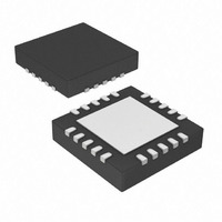
PIC18F13K22-I/ML Microchip Technology, PIC18F13K22-I/ML Datasheet - Page 239

PIC18F13K22-I/ML
Manufacturer Part Number
PIC18F13K22-I/ML
Description
IC MCU 8BIT 8KB FLASH 20-QFN
Manufacturer
Microchip Technology
Series
PIC® XLP™ 18Fr
Datasheets
1.PIC18LF13K22-ISS.pdf
(388 pages)
2.PIC18LF13K22-ISS.pdf
(12 pages)
3.PIC18F13K22-ISS.pdf
(382 pages)
Specifications of PIC18F13K22-I/ML
Program Memory Type
FLASH
Program Memory Size
8KB (4K x 16)
Package / Case
20-VQFN Exposed Pad, 20-HVQFN, 20-SQFN, 20-DHVQFN
Core Processor
PIC
Core Size
8-Bit
Speed
64MHz
Connectivity
I²C, LIN, SPI, UART/USART
Peripherals
Brown-out Detect/Reset, POR, PWM, WDT
Number Of I /o
17
Eeprom Size
256 x 8
Ram Size
256 x 8
Voltage - Supply (vcc/vdd)
1.8 V ~ 5.5 V
Data Converters
A/D 12x10b
Oscillator Type
Internal
Operating Temperature
-40°C ~ 85°C
Processor Series
PIC18F
Core
PIC
Data Bus Width
8 bit
Data Ram Size
256 B
Interface Type
I2C, MSSP, SPI, USART
Maximum Clock Frequency
64 MHz
Number Of Programmable I/os
17
Number Of Timers
4
Operating Supply Voltage
1.8 V to 5.5 V
Maximum Operating Temperature
+ 125 C
Mounting Style
SMD/SMT
3rd Party Development Tools
52715-96, 52716-328, 52717-734, 52712-325, EWPIC18
Development Tools By Supplier
PG164130, DV164035, DV244005, DV164005
Minimum Operating Temperature
- 40 C
On-chip Adc
10 bit, 12 Channel
Lead Free Status / RoHS Status
Lead free / RoHS Compliant
Lead Free Status / RoHS Status
Lead free / RoHS Compliant, Lead free / RoHS Compliant
Available stocks
Company
Part Number
Manufacturer
Quantity
Price
Company:
Part Number:
PIC18F13K22-I/ML
Manufacturer:
SML
Quantity:
20 000
Part Number:
PIC18F13K22-I/ML
Manufacturer:
MICROCHIP/微芯
Quantity:
20 000
- Current page: 239 of 382
- Download datasheet (6Mb)
20.0
There are two independent voltage references
available:
• Programmable Voltage Reference
• 1.024V Fixed Voltage Reference
20.1
The voltage reference module provides an internally
generated voltage reference for the comparators and
the DAC module. The following features are available:
• Independent from comparator operation
• Single 32-level voltage ranges
• Output clamped to V
• Ratiometric with V
• 1.024V Fixed Voltage Reference (FVR)
The VREFCON1 register (Register 20-2) controls the
Voltage Reference module shown in Figure 20-1.
20.1.1
The
comparator configuration. Setting the D1EN bit of the
VREFCON1 register will enable the voltage reference
by allowing current to flow in the V
When the D1EN bit is cleared, current flow in the V
voltage divider is disabled minimizing the power drain
of the voltage reference peripheral.
20.1.2
The
ranges. The 32 levels are set with the DAC1R<4:0>
bits of the VREFCON2 register.
The V
equations:
EQUATION 20-1:
20.1.3
The V
power consumption by setting the D1EN bit of the
VREFCON1 register to ‘0’: This allows the comparator
to detect a zero-crossing while not consuming
additional V
© 2009 Microchip Technology Inc.
V
OUT
V
V
SOURCE
SOURCE
V
voltage
REF
REF
= (V
REF
+ V
VOLTAGE REFERENCES
Voltage Reference
SOURCE
output voltage is determined by the following
+ = V
- = V
output voltage can be set to Vss with no
REF
INDEPENDENT OPERATION
OUTPUT VOLTAGE SELECTION
OUTPUT CLAMPED TO V
SOURCE
voltage reference has 32 voltage level
SS
reference
module current.
DD
+ - V
, or V
, V
-
DD
REF
V
SS
SOURCE
REF
REF
+, or FVR
-
is
OUTPUT VOLTAGE
-)*(DAC1R<4:0>/(2^5))
independent
REF
voltage divider.
SS
of
REF
Preliminary
the
PIC18F1XK22/LF1XK22
20.1.4
The comparator voltage reference is V
therefore, the V
V
Voltage Reference can be found in Section 25.0
“Electrical Specifications”.
20.1.5
The V
CV
VREFCON1 register to ‘1’. Selecting the reference volt-
age for output on the V
the digital output buffer and digital input threshold
detector functions of that pin. Reading the CV
when it has been configured for reference voltage out-
put will always return a ‘0’.
Due to the limited current drive capability, a buffer must
be used on the voltage reference output for external
connections to CV
buffering technique.
20.1.6
When the device wakes up from Sleep through an
interrupt or a Watchdog Timer time-out, the contents of
the RECON1 register are not affected. To minimize
current consumption in Sleep mode, the voltage
reference should be disabled.
20.1.7
A device Reset affects the following:
• Voltage reference is disabled
• Fixed voltage reference is disabled
• V
• The DAC1R<4:0> range select bits are cleared
20.2
The FVR is a stable fixed voltage reference,
independent of V
1.024V. This reference can be enabled by setting the
FVR1EN bit of the VREFCON0 register to ‘1’. The FVR
can be routed to the comparators or an ADC input
channel.
20.2.1
When the Fixed Voltage Reference module is enabled, it
will require some time for the reference and its amplifier
circuits to stabilize. The user program must include a
small delay routine to allow the module to settle. The
FVR1ST stable bit of the VREFCON0 register also
indicates that the FVR has been operating long enough
to
Specifications” for the minimum delay requirement.
DD
REF
REF
. The tested absolute accuracy of the Comparator
be
REF
is removed from the CV
pin by setting the DAC1OE bit of the
FVR Reference Module
voltage reference can be output to the device
stable.
OUTPUT RATIOMETRIC TO V
VOLTAGE REFERENCE OUTPUT
OPERATION DURING SLEEP
EFFECTS OF A RESET
FVR STABILIZATION PERIOD
REF
DD
REF
output changes with fluctuations in
See
, with a nominal output voltage of
. Figure 20-2 shows an example
REF
Section 25.0
pin automatically overrides
REF
DS41365B-page 237
pin
DD
derived and
“Electrical
DD
REF
pin
Related parts for PIC18F13K22-I/ML
Image
Part Number
Description
Manufacturer
Datasheet
Request
R

Part Number:
Description:
Manufacturer:
Microchip Technology Inc.
Datasheet:

Part Number:
Description:
Manufacturer:
Microchip Technology Inc.
Datasheet:

Part Number:
Description:
Manufacturer:
Microchip Technology Inc.
Datasheet:

Part Number:
Description:
Manufacturer:
Microchip Technology Inc.
Datasheet:

Part Number:
Description:
Manufacturer:
Microchip Technology Inc.
Datasheet:

Part Number:
Description:
Manufacturer:
Microchip Technology Inc.
Datasheet:

Part Number:
Description:
Manufacturer:
Microchip Technology Inc.
Datasheet:

Part Number:
Description:
Manufacturer:
Microchip Technology Inc.
Datasheet:


