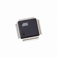
AT91SAM7S32B-AU Atmel, AT91SAM7S32B-AU Datasheet - Page 113

AT91SAM7S32B-AU
Manufacturer Part Number
AT91SAM7S32B-AU
Description
IC MCU ARM7 32KB FLASH 48LQFP
Manufacturer
Atmel
Series
AT91SAMr
Datasheet
1.AT91SAM7S16-MU.pdf
(779 pages)
Specifications of AT91SAM7S32B-AU
Core Processor
ARM7
Core Size
16/32-Bit
Speed
55MHz
Connectivity
I²C, SPI, SSC, UART/USART
Peripherals
Brown-out Detect/Reset, DMA, POR, PWM, WDT
Number Of I /o
21
Program Memory Size
32KB (32K x 8)
Program Memory Type
FLASH
Ram Size
8K x 8
Voltage - Supply (vcc/vdd)
1.65 V ~ 1.95 V
Data Converters
A/D 8x10b
Oscillator Type
Internal
Operating Temperature
-40°C ~ 85°C
Package / Case
48-LQFP
Cpu Family
91S
Device Core
ARM7TDMI
Device Core Size
32b
Frequency (max)
55MHz
Interface Type
SPI/TWI/USART
Total Internal Ram Size
8KB
# I/os (max)
21
Number Of Timers - General Purpose
3
Operating Supply Voltage (typ)
1.8/3.3V
Operating Supply Voltage (max)
1.95/3.6V
Operating Supply Voltage (min)
1.65/3V
On-chip Adc
8-chx10-bit
Instruction Set Architecture
RISC
Operating Temp Range
-40C to 85C
Operating Temperature Classification
Industrial
Mounting
Surface Mount
Pin Count
48
Package Type
LQFP
Package
48LQFP
Family Name
AT91
Maximum Speed
55 MHz
Operating Supply Voltage
1.8|3.3 V
Data Bus Width
32 Bit
Number Of Programmable I/os
21
Number Of Timers
3
For Use With
AT91SAM-ICE - EMULATOR FOR AT91 ARM7/ARM9AT91SAM7S-EK - KIT EVAL FOR ARM AT91SAM7S
Lead Free Status / RoHS Status
Lead free / RoHS Compliant
Eeprom Size
-
Lead Free Status / Rohs Status
Compliant
Available stocks
Company
Part Number
Manufacturer
Quantity
Price
Part Number:
AT91SAM7S32B-AU
Manufacturer:
MICROCHIP/微芯
Quantity:
20 000
- Current page: 113 of 779
- Download datasheet (11Mb)
19.2.4.4
19.2.4.5
6175K–ATARM–30-Aug-10
General-purpose NVM Bits
Security Bit
General-purpose NVM bits do not interfere with the embedded Flash memory plane. (Does not
apply to EFC1 on the AT91SAM7S512.) These general-purpose bits are dedicated to protect
other parts of the product. They can be set (activated) or cleared individually. Refer to the prod-
uct definition section for the general-purpose NVM bit action.
The activation sequence is:
Two errors can be detected in the MC_FSR register after a programming sequence:
It is possible to deactivate a general-purpose NVM bit set previously. The clear sequence is:
Two errors can be detected in the MC_FSR register after a programming sequence:
The Clear General-purpose Bit command programs the general-purpose NVM bit to 0; the corre-
sponding bit GPNVM0 to GPNVMx in MC_FSR reads 0. The Set General-purpose Bit command
programs the general-purpose NVM bit to 1; the corresponding bit GPNVMx in MC_FSR reads 1.
Note:
The goal of the security bit is to prevent external access to the internal bus system. (Does not
apply to EFC1 on the AT91SAM7S512.) JTAG, Fast Flash Programming and Flash Serial Test
Interface features are disabled. Once set, this bit can be reset only by an external hardware
ERASE request to the chip. Refer to the product definition section for the pin name that controls
the ERASE. In this case, the full memory plane is erased and all lock and general-purpose NVM
bits are cleared. The security bit in the MC_FSR is cleared only after these operations. The acti-
vation sequence is:
• Start the Set General Purpose Bit command (SGPB) by writing the Flash Command Register
• When the bit is set, the bit FRDY in the Flash Programming Status Register (MC_FSR) rises.
• Programming Error: A bad keyword and/or an invalid command have been written in the
• If the general-purpose bit number is greater than the total number of general-purpose bits,
• Start the Clear General-purpose Bit command (CGPB) by writing the Flash Command
• When the clear completes, the bit FRDY in the Flash Programming Status Register
• Programming Error: a bad keyword and/or an invalid command have been written in the
• If the number of the general-purpose bit set in the PAGEN field is greater than the total
• Start the Set Security Bit command (SSB) by writing the Flash Command Register.
with the SEL command and the number of the general-purpose bit to be set in the PAGEN
field.
If an interrupt has been enabled by setting the bit FRDY in MC_FMR, the interrupt line of the
Memory Controller is activated.
MC_FCR register
then the command has no effect.
Register with CGPB and the number of the general-purpose bit to be cleared in the PAGEN
field.
(MC_FSR) rises. If an interrupt has been enabled by setting the bit FRDY in MC_FMR, the
interrupt line of the Memory Controller is activated.
MC_FCR register
number of general-purpose bits, then the command has no effect.
Access to the Flash in read mode is permitted when a Set, Clear or Get General-purpose NVM Bit
command is performed.
AT91SAM7S Series Preliminary
113
Related parts for AT91SAM7S32B-AU
Image
Part Number
Description
Manufacturer
Datasheet
Request
R

Part Number:
Description:
KIT EVAL FOR ARM AT91SAM7S
Manufacturer:
Atmel
Datasheet:

Part Number:
Description:
MCU, MPU & DSP Development Tools KICKSTART KIT ATMEL AT91SAM7S
Manufacturer:
IAR Systems

Part Number:
Description:
DEV KIT FOR AVR/AVR32
Manufacturer:
Atmel
Datasheet:

Part Number:
Description:
INTERVAL AND WIPE/WASH WIPER CONTROL IC WITH DELAY
Manufacturer:
ATMEL Corporation
Datasheet:

Part Number:
Description:
Low-Voltage Voice-Switched IC for Hands-Free Operation
Manufacturer:
ATMEL Corporation
Datasheet:

Part Number:
Description:
MONOLITHIC INTEGRATED FEATUREPHONE CIRCUIT
Manufacturer:
ATMEL Corporation
Datasheet:

Part Number:
Description:
AM-FM Receiver IC U4255BM-M
Manufacturer:
ATMEL Corporation
Datasheet:

Part Number:
Description:
Monolithic Integrated Feature Phone Circuit
Manufacturer:
ATMEL Corporation
Datasheet:

Part Number:
Description:
Multistandard Video-IF and Quasi Parallel Sound Processing
Manufacturer:
ATMEL Corporation
Datasheet:

Part Number:
Description:
High-performance EE PLD
Manufacturer:
ATMEL Corporation
Datasheet:

Part Number:
Description:
8-bit Flash Microcontroller
Manufacturer:
ATMEL Corporation
Datasheet:

Part Number:
Description:
2-Wire Serial EEPROM
Manufacturer:
ATMEL Corporation
Datasheet:


