AT91SAM7S32B-AU Atmel, AT91SAM7S32B-AU Datasheet - Page 597
AT91SAM7S32B-AU
Manufacturer Part Number
AT91SAM7S32B-AU
Description
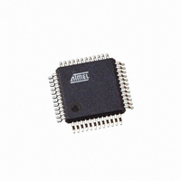
IC MCU ARM7 32KB FLASH 48LQFP
Manufacturer
Atmel
Series
AT91SAMr
Datasheet
1.AT91SAM7S16-MU.pdf
(779 pages)
Specifications of AT91SAM7S32B-AU
Core Processor
ARM7
Core Size
16/32-Bit
Speed
55MHz
Connectivity
I²C, SPI, SSC, UART/USART
Peripherals
Brown-out Detect/Reset, DMA, POR, PWM, WDT
Number Of I /o
21
Program Memory Size
32KB (32K x 8)
Program Memory Type
FLASH
Ram Size
8K x 8
Voltage - Supply (vcc/vdd)
1.65 V ~ 1.95 V
Data Converters
A/D 8x10b
Oscillator Type
Internal
Operating Temperature
-40°C ~ 85°C
Package / Case
48-LQFP
Cpu Family
91S
Device Core
ARM7TDMI
Device Core Size
32b
Frequency (max)
55MHz
Interface Type
SPI/TWI/USART
Total Internal Ram Size
8KB
# I/os (max)
21
Number Of Timers - General Purpose
3
Operating Supply Voltage (typ)
1.8/3.3V
Operating Supply Voltage (max)
1.95/3.6V
Operating Supply Voltage (min)
1.65/3V
On-chip Adc
8-chx10-bit
Instruction Set Architecture
RISC
Operating Temp Range
-40C to 85C
Operating Temperature Classification
Industrial
Mounting
Surface Mount
Pin Count
48
Package Type
LQFP
Package
48LQFP
Family Name
AT91
Maximum Speed
55 MHz
Operating Supply Voltage
1.8|3.3 V
Data Bus Width
32 Bit
Number Of Programmable I/os
21
Number Of Timers
3
For Use With
AT91SAM-ICE - EMULATOR FOR AT91 ARM7/ARM9AT91SAM7S-EK - KIT EVAL FOR ARM AT91SAM7S
Lead Free Status / RoHS Status
Lead free / RoHS Compliant
Eeprom Size
-
Lead Free Status / Rohs Status
Compliant
Available stocks
Company
Part Number
Manufacturer
Quantity
Price

Part Number:
AT91SAM7S32B-AU
Manufacturer:
MICROCHIP/微芯
Quantity:
20 000


40.4.2
40.4.2.1
40.4.3
40.4.3.1
40.4.3.2
6175K–ATARM–30-Aug-10
Embedded Flash Controller (EFC)
Parallel Input/Output Controller (PIO)
EFC: Embedded Flash Access Time 1
PIO: Leakage on PA17 - PA20
PIO: Electrical Characteristics on NRST and PA0-PA16 and PA21-31
To activate sleep mode as soon as possible, it is recommended to write successively, ADC
Mode Register (SLEEP) then ADC Control Register (START bit field); to start an analog-to-digi-
tal conversion, in order put ADC into sleep mode at the end of this conversion.
The embedded Flash maximum access time is 20 MHz (instead of 30 MHz) at zero Wait State
(FWS = 0).
The maximum operating frequency with one Wait State (FWS = 1) is 48.1 MHz (instead of 55
MHz). Above 48.1 MHz and until 55 MHz, two Wait States (FWS = 2) are required.
Set the number of Wait States (FWS) according to the frequency requirements described in this
errata.
When PA17, PA18, PA19 or PA20 (the I/O lines multiplexed with the analog inputs) are set as
digital inputs with pull-up disabled, the leakage can be 9 µA in worst case and 90 nA in typical
case per I/O when the I/O is set externally at low level.
Set the I/O to VDDIO by internal or external pull-up.
When NRST or PA0-PA16 or PA21-PA31 are set as digital inputs with pull-up enabled, the volt-
age of the I/O stabilizes at VPull-up.
Vpull-up
This condition causes a leakage through VDDIO. This leakage is 45 µA per pad in worst case at
3.3 V and 25 µA at 1.8V.
I Leakage
It is recommended to use an external pull-up if needed.
VPull-up Min
VDDIO - 0.65 V
Parameter
I Leakage at 3,3V
I Leakage at 1.8V
Problem Fix/Workaround
Problem Fix/Workaround
Problem Fix/Workaround
Problem Fix/Workaround
VPull-up Max
VDDIO - 0.45 V
Typ
2.5
1
µA
µA
Max
45
25
AT91SAM7S Series Preliminary
µA
µA
597
Related parts for AT91SAM7S32B-AU
Image
Part Number
Description
Manufacturer
Datasheet
Request
R

Part Number:
Description:
KIT EVAL FOR ARM AT91SAM7S
Manufacturer:
Atmel
Datasheet:

Part Number:
Description:
MCU, MPU & DSP Development Tools KICKSTART KIT ATMEL AT91SAM7S
Manufacturer:
IAR Systems

Part Number:
Description:
DEV KIT FOR AVR/AVR32
Manufacturer:
Atmel
Datasheet:

Part Number:
Description:
INTERVAL AND WIPE/WASH WIPER CONTROL IC WITH DELAY
Manufacturer:
ATMEL Corporation
Datasheet:
Part Number:
Description:
Low-Voltage Voice-Switched IC for Hands-Free Operation
Manufacturer:
ATMEL Corporation
Datasheet:
Part Number:
Description:
MONOLITHIC INTEGRATED FEATUREPHONE CIRCUIT
Manufacturer:
ATMEL Corporation
Datasheet:
Part Number:
Description:
AM-FM Receiver IC U4255BM-M
Manufacturer:
ATMEL Corporation
Datasheet:
Part Number:
Description:
Monolithic Integrated Feature Phone Circuit
Manufacturer:
ATMEL Corporation
Datasheet:
Part Number:
Description:
Multistandard Video-IF and Quasi Parallel Sound Processing
Manufacturer:
ATMEL Corporation
Datasheet:
Part Number:
Description:
High-performance EE PLD
Manufacturer:
ATMEL Corporation
Datasheet:
Part Number:
Description:
8-bit Flash Microcontroller
Manufacturer:
ATMEL Corporation
Datasheet:
Part Number:
Description:
2-Wire Serial EEPROM
Manufacturer:
ATMEL Corporation
Datasheet: