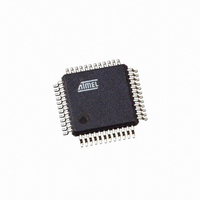
AT91SAM7S32B-AU Atmel, AT91SAM7S32B-AU Datasheet - Page 333

AT91SAM7S32B-AU
Manufacturer Part Number
AT91SAM7S32B-AU
Description
IC MCU ARM7 32KB FLASH 48LQFP
Manufacturer
Atmel
Series
AT91SAMr
Datasheet
1.AT91SAM7S16-MU.pdf
(779 pages)
Specifications of AT91SAM7S32B-AU
Core Processor
ARM7
Core Size
16/32-Bit
Speed
55MHz
Connectivity
I²C, SPI, SSC, UART/USART
Peripherals
Brown-out Detect/Reset, DMA, POR, PWM, WDT
Number Of I /o
21
Program Memory Size
32KB (32K x 8)
Program Memory Type
FLASH
Ram Size
8K x 8
Voltage - Supply (vcc/vdd)
1.65 V ~ 1.95 V
Data Converters
A/D 8x10b
Oscillator Type
Internal
Operating Temperature
-40°C ~ 85°C
Package / Case
48-LQFP
Cpu Family
91S
Device Core
ARM7TDMI
Device Core Size
32b
Frequency (max)
55MHz
Interface Type
SPI/TWI/USART
Total Internal Ram Size
8KB
# I/os (max)
21
Number Of Timers - General Purpose
3
Operating Supply Voltage (typ)
1.8/3.3V
Operating Supply Voltage (max)
1.95/3.6V
Operating Supply Voltage (min)
1.65/3V
On-chip Adc
8-chx10-bit
Instruction Set Architecture
RISC
Operating Temp Range
-40C to 85C
Operating Temperature Classification
Industrial
Mounting
Surface Mount
Pin Count
48
Package Type
LQFP
Package
48LQFP
Family Name
AT91
Maximum Speed
55 MHz
Operating Supply Voltage
1.8|3.3 V
Data Bus Width
32 Bit
Number Of Programmable I/os
21
Number Of Timers
3
For Use With
AT91SAM-ICE - EMULATOR FOR AT91 ARM7/ARM9AT91SAM7S-EK - KIT EVAL FOR ARM AT91SAM7S
Lead Free Status / RoHS Status
Lead free / RoHS Compliant
Eeprom Size
-
Lead Free Status / Rohs Status
Compliant
Available stocks
Company
Part Number
Manufacturer
Quantity
Price
Part Number:
AT91SAM7S32B-AU
Manufacturer:
MICROCHIP/微芯
Quantity:
20 000
- Current page: 333 of 779
- Download datasheet (11Mb)
30.9
30.9.1
30.9.2
30.9.3
30.9.4
30.9.4.1
6175K–ATARM–30-Aug-10
Slave Mode
Definition
Application Block Diagram
Programming Slave Mode
Receiving Data
Read Sequence
The Slave Mode is defined as a mode where the device receives the clock and the address from
another device called the master.
In this mode, the device never initiates and never completes the transmission (START,
REPEATED_START and STOP conditions are always provided by the master).
Figure 30-23. Slave Mode Typical Application Block Diagram
The following fields must be programmed before entering Slave mode:
As the device receives the clock, values written in TWI_CWGR are not taken into account.
After a Start or Repeated Start condition is detected and if the address sent by the Master
matches with the Slave address programmed in the SADR (Slave ADdress) field, SVACC (Slave
ACCess) flag is set and SVREAD (Slave READ) indicates the direction of the transfer.
SVACC remains high until a STOP condition or a repeated START is detected. When such a
condition is detected, EOSACC (End Of Slave ACCess) flag is set.
In the case of a Read sequence (SVREAD is high), TWI transfers data written in the TWI_THR
(TWI Transmit Holding Register) until a STOP condition or a REPEATED_START + an address
different from SADR is detected. Note that at the end of the read sequence TXCOMP (Transmis-
sion Complete) flag is set and SVACC reset.
As soon as data is written in the TWI_THR, TXRDY (Transmit Holding Register Ready) flag is
reset, and it is set when the shift register is empty and the sent data acknowledged or not. If the
data is not acknowledged, the NACK flag is set.
1. SADR (TWI_SMR): The slave device address is used in order to be accessed by mas-
2. MSDIS (TWI_CR): Disable the master mode.
3. SVEN (TWI_CR): Enable the slave mode.
Host with
Interface
Master
ter devices in read or write mode.
TWI
TWD
TWCK
Host with TWI
Interface
Slave 1
AT91SAM7S Series Preliminary
Host with TWI
Interface
Slave 2
LCD Controller
Slave 3
R
R
VDD
333
Related parts for AT91SAM7S32B-AU
Image
Part Number
Description
Manufacturer
Datasheet
Request
R

Part Number:
Description:
KIT EVAL FOR ARM AT91SAM7S
Manufacturer:
Atmel
Datasheet:

Part Number:
Description:
MCU, MPU & DSP Development Tools KICKSTART KIT ATMEL AT91SAM7S
Manufacturer:
IAR Systems

Part Number:
Description:
DEV KIT FOR AVR/AVR32
Manufacturer:
Atmel
Datasheet:

Part Number:
Description:
INTERVAL AND WIPE/WASH WIPER CONTROL IC WITH DELAY
Manufacturer:
ATMEL Corporation
Datasheet:

Part Number:
Description:
Low-Voltage Voice-Switched IC for Hands-Free Operation
Manufacturer:
ATMEL Corporation
Datasheet:

Part Number:
Description:
MONOLITHIC INTEGRATED FEATUREPHONE CIRCUIT
Manufacturer:
ATMEL Corporation
Datasheet:

Part Number:
Description:
AM-FM Receiver IC U4255BM-M
Manufacturer:
ATMEL Corporation
Datasheet:

Part Number:
Description:
Monolithic Integrated Feature Phone Circuit
Manufacturer:
ATMEL Corporation
Datasheet:

Part Number:
Description:
Multistandard Video-IF and Quasi Parallel Sound Processing
Manufacturer:
ATMEL Corporation
Datasheet:

Part Number:
Description:
High-performance EE PLD
Manufacturer:
ATMEL Corporation
Datasheet:

Part Number:
Description:
8-bit Flash Microcontroller
Manufacturer:
ATMEL Corporation
Datasheet:

Part Number:
Description:
2-Wire Serial EEPROM
Manufacturer:
ATMEL Corporation
Datasheet:


