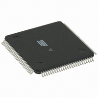
ATXMEGA64A1-AU Atmel, ATXMEGA64A1-AU Datasheet - Page 5

ATXMEGA64A1-AU
Manufacturer Part Number
ATXMEGA64A1-AU
Description
MCU AVR 64K FLASH 1.6V 100-TQFP
Manufacturer
Atmel
Series
AVR® XMEGAr
Datasheet
1.ATAVRONEKIT.pdf
(113 pages)
Specifications of ATXMEGA64A1-AU
Core Processor
AVR
Core Size
8/16-Bit
Speed
32MHz
Connectivity
EBI/EMI, I²C, IrDA, SPI, UART/USART
Peripherals
Brown-out Detect/Reset, DMA, POR, PWM, WDT
Number Of I /o
78
Program Memory Size
64KB (32K x 16)
Program Memory Type
FLASH
Eeprom Size
2K x 8
Ram Size
4K x 8
Voltage - Supply (vcc/vdd)
1.6 V ~ 3.6 V
Data Converters
A/D 16x12b, D/A 4x12b
Oscillator Type
Internal
Operating Temperature
-40°C ~ 85°C
Package / Case
100-TQFP, 100-VQFP
Processor Series
ATXMEGA64x
Core
AVR8
Data Bus Width
8 bit, 16 bit
Data Ram Size
4 KB
Interface Type
I2C/SPI/USART
Maximum Clock Frequency
32 MHz
Number Of Programmable I/os
78
Number Of Timers
8
Operating Supply Voltage
1.6 V to 3.6 V
Maximum Operating Temperature
+ 85 C
Mounting Style
SMD/SMT
3rd Party Development Tools
EWAVR, EWAVR-BL
Development Tools By Supplier
ATAVRDRAGON, ATAVRISP2, ATAVRONEKIT
Minimum Operating Temperature
- 40 C
On-chip Adc
2 (8-ch x 12-bit)
On-chip Dac
2 (2-ch x 12-bit)
Package
100TQFP
Device Core
AVR
Family Name
XMEGA
Maximum Speed
32 MHz
For Use With
ATAVRONEKIT - KIT AVR/AVR32 DEBUGGER/PROGRMMRATSTK600-TQFP100 - STK600 SOCKET/ADAPTER 100-TQFPATSTK600-TQFP44 - STK600 SOCKET/ADAPTER 44-TQFP770-1007 - ISP 4PORT ATMEL AVR MCU SPI/JTAG770-1004 - ISP 4PORT FOR ATMEL AVR MCU SPIATAVRISP2 - PROGRAMMER AVR IN SYSTEM
Lead Free Status / RoHS Status
Lead free / RoHS Compliant
Available stocks
Company
Part Number
Manufacturer
Quantity
Price
Company:
Part Number:
ATXMEGA64A1-AU
Manufacturer:
Atmel
Quantity:
135
3. Overview
8067M–AVR–09/10
The Atmel
CMOS 8/16-bit microcontrollers based on the AVR enhanced RISC architecture. By executing
powerful instructions in a single clock cycle, the XMEGA A1 achieves throughputs approaching
1 Million Instructions Per Second (MIPS) per MHz allowing the system designer to optimize
power consumption versus processing speed.
The AVR CPU combines a rich instruction set with 32 general purpose working registers. All the
32 registers are directly connected to the Arithmetic Logic Unit (ALU), allowing two independent
registers to be accessed in one single instruction, executed in one clock cycle. The resulting
architecture is more code efficient while achieving throughputs many times faster than conven-
tional single-accumulator or CISC based microcontrollers.
The XMEGA A1 devices provides the following features: In-System Programmable Flash with
Read-While-Write capabilities, Internal EEPROM and SRAM, four-channel DMA Controller,
eight-channel Event System, Programmable Multi-level Interrupt Controller, 78 general purpose
I/O lines, 16-bit Real Time Counter (RTC), eight flexible 16-bit Timer/Counters with compare
modes and PWM, eight USARTs, four Two Wire Serial Interfaces (TWIs), four Serial Peripheral
Interfaces (SPIs), AES and DES crypto engine, two 8-channel, 12-bit ADCs with optional differ-
ential input with programmable gain, two 2-channel, 12-bit DACs, four analog comparators with
window mode, programmable Watchdog Timer with seperate Internal Oscillator, accurate inter-
nal oscillators with PLL and prescaler and programmable Brown-Out Detection.
The Program and Debug Interface (PDI), a fast 2-pin interface for programming and debugging,
is available. The devices also have an IEEE std. 1149.1 compliant JTAG test interface, and this
can also be used for On-chip Debug and programming.
The XMEGA A1 devices have five software selectable power saving modes. The Idle mode
stops the CPU while allowing the SRAM, DMA Controller, Event System, Interrupt Controller and
all peripherals to continue functioning. The Power-down mode saves the SRAM and register
contents but stops the oscillators, disabling all other functions until the next TWI or pin-change
interrupt, or Reset. In Power-save mode, the asynchronous Real Time Counter continues to run,
allowing the application to maintain a timer base while the rest of the device is sleeping. In
Standby mode, the Crystal/Resonator Oscillator is kept running while the rest of the device is
sleeping. This allows very fast start-up from external crystal combined with low power consump-
tion. In Extended Standby mode, both the main Oscillator and the Asynchronous Timer continue
to run. To further reduce power consumption, the peripheral clock to each individual peripheral
can optionally be stopped in Active mode and Idle sleep mode.
The device is manufactured using Atmel's high-density nonvolatile memory technology. The pro-
gram Flash memory can be reprogrammed in-system through the PDI or JTAG. A Bootloader
running in the device can use any interface to download the application program to the Flash
memory. The Bootloader software in the Boot Flash section will continue to run while the Appli-
cation Flash section is updated, providing true Read-While-Write operation. By combining an
8/16-bit RISC CPU with In-System Self-Programmable Flash, the Atmel XMEGA A1 is a power-
ful microcontroller family that provides a highly flexible and cost effective solution for many
embedded applications.
The XMEGA A1 devices are supported with a full suite of program and system development
tools including: C compilers, macro assemblers, program debugger/simulators, programmers,
and evaluation kits.
®
AVR
®
XMEGA
™
A1 is a family of low power, high performance and peripheral rich
XMEGA A1
5


