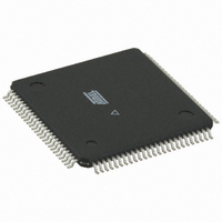
ATXMEGA64A1-AU Atmel, ATXMEGA64A1-AU Datasheet - Page 8

ATXMEGA64A1-AU
Manufacturer Part Number
ATXMEGA64A1-AU
Description
MCU AVR 64K FLASH 1.6V 100-TQFP
Manufacturer
Atmel
Series
AVR® XMEGAr
Datasheet
1.ATAVRONEKIT.pdf
(113 pages)
Specifications of ATXMEGA64A1-AU
Core Processor
AVR
Core Size
8/16-Bit
Speed
32MHz
Connectivity
EBI/EMI, I²C, IrDA, SPI, UART/USART
Peripherals
Brown-out Detect/Reset, DMA, POR, PWM, WDT
Number Of I /o
78
Program Memory Size
64KB (32K x 16)
Program Memory Type
FLASH
Eeprom Size
2K x 8
Ram Size
4K x 8
Voltage - Supply (vcc/vdd)
1.6 V ~ 3.6 V
Data Converters
A/D 16x12b, D/A 4x12b
Oscillator Type
Internal
Operating Temperature
-40°C ~ 85°C
Package / Case
100-TQFP, 100-VQFP
Processor Series
ATXMEGA64x
Core
AVR8
Data Bus Width
8 bit, 16 bit
Data Ram Size
4 KB
Interface Type
I2C/SPI/USART
Maximum Clock Frequency
32 MHz
Number Of Programmable I/os
78
Number Of Timers
8
Operating Supply Voltage
1.6 V to 3.6 V
Maximum Operating Temperature
+ 85 C
Mounting Style
SMD/SMT
3rd Party Development Tools
EWAVR, EWAVR-BL
Development Tools By Supplier
ATAVRDRAGON, ATAVRISP2, ATAVRONEKIT
Minimum Operating Temperature
- 40 C
On-chip Adc
2 (8-ch x 12-bit)
On-chip Dac
2 (2-ch x 12-bit)
Package
100TQFP
Device Core
AVR
Family Name
XMEGA
Maximum Speed
32 MHz
For Use With
ATAVRONEKIT - KIT AVR/AVR32 DEBUGGER/PROGRMMRATSTK600-TQFP100 - STK600 SOCKET/ADAPTER 100-TQFPATSTK600-TQFP44 - STK600 SOCKET/ADAPTER 44-TQFP770-1007 - ISP 4PORT ATMEL AVR MCU SPI/JTAG770-1004 - ISP 4PORT FOR ATMEL AVR MCU SPIATAVRISP2 - PROGRAMMER AVR IN SYSTEM
Lead Free Status / RoHS Status
Lead free / RoHS Compliant
Available stocks
Company
Part Number
Manufacturer
Quantity
Price
Company:
Part Number:
ATXMEGA64A1-AU
Manufacturer:
Atmel
Quantity:
135
6. AVR CPU
6.1
6.2
8067M–AVR–09/10
Features
Overview
•
•
•
•
•
•
•
•
The XMEGA A1 uses the 8/16-bit AVR CPU. The main function of the CPU is program execu-
tion. The CPU must therefore be able to access memories, perform calculations and control
peripherals. Interrupt handling is described in a separate section.
the CPU block diagram.
Figure 6-1.
The AVR uses a Harvard architecture - with separate memories and buses for program and
data. Instructions in the program memory are executed with a single level pipeline. While one
instruction is being executed, the next instruction is pre-fetched from the program memory. This
8/16-bit high performance AVR RISC Architecture
32x8-bit registers directly connected to the ALU
Stack in SRAM
Stack Pointer accessible in I/O memory space
Direct addressing of up to 16M Bytes of program and data memory
True 16/24-bit access to 16/24-bit I/O registers
Support for 8-, 16- and 32-bit Arithmetic
Configuration Change Protection of system critical features
– 138 instructions
– Hardware multiplier
Peripheral
Module 1
CPU block diagram
CONTROL
STATUS/
Program
Counter
OCD
Peripheral
Module 2
Instruction
Instruction
Program
Register
Memory
Decode
Flash
DATA BUS
SRAM
DATA BUS
ALU
EEPROM
32 x 8 General
Registers
Multiplier/
Purpose
DES
Figure 6-1 on page 8
PMIC
XMEGA A1
shows
8


