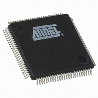
AT91M40800-33AU Atmel, AT91M40800-33AU Datasheet - Page 18

AT91M40800-33AU
Manufacturer Part Number
AT91M40800-33AU
Description
IC ARM7 MCU 100 LQFP
Manufacturer
Atmel
Series
AT91SAMr
Specifications of AT91M40800-33AU
Core Processor
ARM7
Core Size
16/32-Bit
Speed
33MHz
Connectivity
EBI/EMI, UART/USART
Peripherals
POR, WDT
Number Of I /o
32
Program Memory Type
ROMless
Ram Size
8K x 8
Voltage - Supply (vcc/vdd)
1.8 V ~ 3.6 V
Oscillator Type
External
Operating Temperature
-40°C ~ 85°C
Package / Case
100-LQFP
Package
100TQFP
Device Core
ARM7TDMI
Family Name
91M
Maximum Speed
33 MHz
Operating Supply Voltage
2.5|3.3 V
Data Bus Width
32 Bit
Number Of Programmable I/os
32
Interface Type
EBI/USART
Number Of Timers
3
Processor Series
AT91Mx
Core
ARM7TDMI
Data Ram Size
8 KB
Maximum Clock Frequency
33 MHz
Maximum Operating Temperature
+ 85 C
Mounting Style
SMD/SMT
3rd Party Development Tools
JTRACE-ARM-2M, MDK-ARM, RL-ARM, ULINK2
Minimum Operating Temperature
- 40 C
Eeprom Memory
0 Bytes
Input Output
32
Interface
EBI/EMI, UART/USART
Ios
32
Memory Type
ROMless
Number Of Bits
32
Package Type
100-pin LQFP
Programmable Memory
0 Bytes
Timers
3-16-bit
Voltage, Range
1.8-3.6 V
Cpu Family
91M
Device Core Size
32b
Frequency (max)
33MHz
Program Memory Size
Not Required
Total Internal Ram Size
8KB
# I/os (max)
32
Number Of Timers - General Purpose
3
Operating Supply Voltage (typ)
2.5/3.3V
Operating Supply Voltage (max)
3.6V
Operating Supply Voltage (min)
1.8V
Instruction Set Architecture
RISC
Operating Temp Range
-40C to 85C
Operating Temperature Classification
Industrial
Mounting
Surface Mount
Pin Count
100
Lead Free Status / RoHS Status
Lead free / RoHS Compliant
Eeprom Size
-
Program Memory Size
-
Data Converters
-
Lead Free Status / Rohs Status
Lead free / RoHS Compliant
Available stocks
Company
Part Number
Manufacturer
Quantity
Price
Company:
Part Number:
AT91M40800-33AU
Manufacturer:
ATMEL
Quantity:
1 000
Company:
Part Number:
AT91M40800-33AU
Manufacturer:
ATMEL
Quantity:
346
Part Number:
AT91M40800-33AU
Manufacturer:
ATMEL/爱特梅尔
Quantity:
20 000
EBI: External Bus
Interface
External Memory
Mapping
18
AT91X40 Series
The EBI generates the signals that control the access to the external memory or periph-
eral devices. The EBI is fully-programmable and can address up to 64M bytes. It has
eight chip selects and a 24-bit address bus, the upper four bits of which are multiplexed
with a chip select.
The 16-bit data bus can be configured to interface with 8- or 16-bit external devices.
Separate read and write control signals allow for direct memory and peripheral
interfacing.
The EBI supports different access protocols allowing single-clock cycle memory
accesses.
The main features are:
•
•
•
•
•
•
•
•
•
The “EBI User Interface” is described on page 45.
The memory map associates the internal 32-bit address space with the external 24-bit
address bus.
The memory map is defined by programming the base address and page size of the
external memories (see “EBI User Interface” registers EBI_CSR0 to EBI_CSR7). Note
that A0 - A23 is only significant for 8-bit memory; A1 - A23 is used for 16-bit memory.
If the physical memory device is smaller than the programmed page size, it wraps
around and appears to be repeated within the page. The EBI correctly handles any valid
access to the memory device within the page (see Figure 6).
In the event of an access request to an address outside any programmed page, an
Abort signal is generated. Two types of Abort are possible: instruction prefetch abort
and data abort. The corresponding exception vector addresses are respectively
0x0000000C and 0x00000010. It is up to the system programmer to program the error
handling routine to use in case of an Abort (see the ARM7TDMI datasheet for further
information).
If two chip selects are defined as having the same base address, an access to the over-
lapping address space asserts both NCS lines. The Chip Select Register with the
smaller number defines the characteristics of the external access and the behavior of
the control signals.
External memory mapping
Up to 8 chip select lines
8- or 16-bit data bus
Byte write or byte select lines
Remap of boot memory
Two different read protocols
Programmable wait state generation
External wait request
Programmable data float time
1354D–ATARM–08/02


