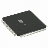
ATMEGA1280V-8AU Atmel, ATMEGA1280V-8AU Datasheet - Page 305

ATMEGA1280V-8AU
Manufacturer Part Number
ATMEGA1280V-8AU
Description
IC MCU AVR 128K FLASH 100-TQFP
Manufacturer
Atmel
Series
AVR® ATmegar
Specifications of ATMEGA1280V-8AU
Core Processor
AVR
Core Size
8-Bit
Speed
8MHz
Connectivity
EBI/EMI, I²C, SPI, UART/USART
Peripherals
Brown-out Detect/Reset, POR, PWM, WDT
Number Of I /o
86
Program Memory Size
128KB (64K x 16)
Program Memory Type
FLASH
Eeprom Size
4K x 8
Ram Size
8K x 8
Voltage - Supply (vcc/vdd)
1.8 V ~ 5.5 V
Data Converters
A/D 16x10b
Oscillator Type
Internal
Operating Temperature
-40°C ~ 85°C
Package / Case
100-TQFP, 100-VQFP
Processor Series
ATMEGA128x
Core
AVR8
Data Bus Width
8 bit
Data Ram Size
8 KB
Interface Type
2-Wire/SPI/USART
Maximum Clock Frequency
8 MHz
Number Of Programmable I/os
86
Number Of Timers
6
Operating Supply Voltage
1.8 V to 5.5 V
Maximum Operating Temperature
+ 85 C
Mounting Style
SMD/SMT
3rd Party Development Tools
EWAVR, EWAVR-BL
Minimum Operating Temperature
- 40 C
On-chip Adc
16-ch x 10-bit
Package
100TQFP
Device Core
AVR
Family Name
ATmega
Maximum Speed
8 MHz
Controller Family/series
AVR MEGA
No. Of I/o's
86
Eeprom Memory Size
4KB
Ram Memory Size
8KB
Cpu Speed
8MHz
Rohs Compliant
Yes
For Use With
ATSTK600-TQFP100 - STK600 SOCKET/ADAPTER 100-TQFP770-1007 - ISP 4PORT ATMEL AVR MCU SPI/JTAG770-1005 - ISP 4PORT FOR ATMEL AVR MCU JTAG770-1004 - ISP 4PORT FOR ATMEL AVR MCU SPIATAVRISP2 - PROGRAMMER AVR IN SYSTEMATSTK503 - STARTER KIT AVR EXP MODULE 100PATJTAGICE2 - AVR ON-CHIP D-BUG SYSTEM
Lead Free Status / RoHS Status
Lead free / RoHS Compliant
Available stocks
Company
Part Number
Manufacturer
Quantity
Price
Part Number:
ATMEGA1280V-8AU
Manufacturer:
ATMEL/爱特梅尔
Quantity:
20 000
- Current page: 305 of 444
- Download datasheet (10Mb)
27.4.3
27.4.4
27.4.5
27.5
27.5.1
2549M–AVR–09/10
Boundary-scan Chain
SAMPLE_PRELOAD; 0x2
AVR_RESET; 0xC
BYPASS; 0xF
Scanning the Digital Port Pins
The active states are:
•
•
Mandatory JTAG instruction for pre-loading the output latches and taking a snap-shot of the
input/output pins without affecting the system operation. However, the output latches are not
connected to the pins. The Boundary-scan Chain is selected as Data Register.
The active states are:
•
•
•
The AVR specific public JTAG instruction for forcing the AVR device into the Reset mode or
releasing the JTAG reset source. The TAP controller is not reset by this instruction. The one bit
Reset Register is selected as Data Register. Note that the reset will be active as long as there is
a logic “one” in the Reset Chain. The output from this chain is not latched.
The active states are:
•
Mandatory JTAG instruction selecting the Bypass Register for Data Register.
The active states are:
•
•
The Boundary-scan chain has the capability of driving and observing the logic levels on the digi-
tal I/O pins, as well as the boundary between digital and analog logic for analog circuitry having
off-chip connection.
Figure 27-3 on page 306
function is disabled during Boundary-scan when the JTAG IC contains EXTEST or
SAMPLE_PRELOAD. The cell consists of a bi-directional pin cell that combines the three sig-
nals Output Control - OCxn, Output Data - ODxn, and Input Data - IDxn, into only a two-stage
Shift Register. The port and pin indexes are not used in the following description.
The Boundary-scan logic is not included in the figures in the datasheet.
shows a simple digital port pin as described in the section
ary-scan details from
307.
When no alternate port function is present, the Input Data - ID - corresponds to the PINxn Regis-
ter value (but ID has no synchronizer), Output Data corresponds to the PORT Register, Output
Capture-DR: Data in the IDCODE Register is sampled into the Boundary-scan Chain.
Shift-DR: The IDCODE scan chain is shifted by the TCK input.
Capture-DR: Data on the external pins are sampled into the Boundary-scan Chain.
Shift-DR: The Boundary-scan Chain is shifted by the TCK input.
Update-DR: Data from the Boundary-scan chain is applied to the output latches. However,
the output latches are not connected to the pins.
Shift-DR: The Reset Register is shifted by the TCK input.
Capture-DR: Loads a logic “0” into the Bypass Register.
Shift-DR: The Bypass Register cell between TDI and TDO is shifted.
Figure 27-3 on page 306
shows the Boundary-scan Cell for a bi-directional port pin. The pull-up
ATmega640/1280/1281/2560/2561
replaces the dashed box in
“I/O-Ports” on page
Figure 27-4 on page 307
Figure 27-4 on page
70. The Bound-
305
Related parts for ATMEGA1280V-8AU
Image
Part Number
Description
Manufacturer
Datasheet
Request
R

Part Number:
Description:
Manufacturer:
ATMEL Corporation
Datasheet:

Part Number:
Description:
Microcontroller with 128K bytes In-system programmable flash, 8 MHz, power supply =2.7 - 5.5V
Manufacturer:
ATMEL Corporation
Datasheet:

Part Number:
Description:
IC AVR MCU 128K 16MHZ 5V 64TQFP
Manufacturer:
Atmel
Datasheet:

Part Number:
Description:
IC AVR MCU 128K 16MHZ 5V 64-QFN
Manufacturer:
Atmel
Datasheet:

Part Number:
Description:
IC AVR MCU 128K 16MHZ COM 64-QFN
Manufacturer:
Atmel
Datasheet:

Part Number:
Description:
IC AVR MCU 128K 16MHZ 64-TQFP
Manufacturer:
Atmel
Datasheet:

Part Number:
Description:
IC AVR MCU 128K 16MHZ 64-TQFP
Manufacturer:
Atmel
Datasheet:

Part Number:
Description:
IC AVR MCU 128K 16MHZ IND 64-QFN
Manufacturer:
Atmel
Datasheet:

Part Number:
Description:
MCU AVR 128KB FLASH 16MHZ 64TQFP
Manufacturer:
Atmel
Datasheet:

Part Number:
Description:
MCU AVR 128KB FLASH 16MHZ 64QFN
Manufacturer:
Atmel
Datasheet:

Part Number:
Description:
MCU AVR 128KB FLASH 16MHZ 64TQFP
Manufacturer:
Atmel
Datasheet:


