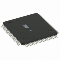
ATMEGA1280V-8AU Atmel, ATMEGA1280V-8AU Datasheet - Page 89

ATMEGA1280V-8AU
Manufacturer Part Number
ATMEGA1280V-8AU
Description
IC MCU AVR 128K FLASH 100-TQFP
Manufacturer
Atmel
Series
AVR® ATmegar
Specifications of ATMEGA1280V-8AU
Core Processor
AVR
Core Size
8-Bit
Speed
8MHz
Connectivity
EBI/EMI, I²C, SPI, UART/USART
Peripherals
Brown-out Detect/Reset, POR, PWM, WDT
Number Of I /o
86
Program Memory Size
128KB (64K x 16)
Program Memory Type
FLASH
Eeprom Size
4K x 8
Ram Size
8K x 8
Voltage - Supply (vcc/vdd)
1.8 V ~ 5.5 V
Data Converters
A/D 16x10b
Oscillator Type
Internal
Operating Temperature
-40°C ~ 85°C
Package / Case
100-TQFP, 100-VQFP
Processor Series
ATMEGA128x
Core
AVR8
Data Bus Width
8 bit
Data Ram Size
8 KB
Interface Type
2-Wire/SPI/USART
Maximum Clock Frequency
8 MHz
Number Of Programmable I/os
86
Number Of Timers
6
Operating Supply Voltage
1.8 V to 5.5 V
Maximum Operating Temperature
+ 85 C
Mounting Style
SMD/SMT
3rd Party Development Tools
EWAVR, EWAVR-BL
Minimum Operating Temperature
- 40 C
On-chip Adc
16-ch x 10-bit
Package
100TQFP
Device Core
AVR
Family Name
ATmega
Maximum Speed
8 MHz
Controller Family/series
AVR MEGA
No. Of I/o's
86
Eeprom Memory Size
4KB
Ram Memory Size
8KB
Cpu Speed
8MHz
Rohs Compliant
Yes
For Use With
ATSTK600-TQFP100 - STK600 SOCKET/ADAPTER 100-TQFP770-1007 - ISP 4PORT ATMEL AVR MCU SPI/JTAG770-1005 - ISP 4PORT FOR ATMEL AVR MCU JTAG770-1004 - ISP 4PORT FOR ATMEL AVR MCU SPIATAVRISP2 - PROGRAMMER AVR IN SYSTEMATSTK503 - STARTER KIT AVR EXP MODULE 100PATJTAGICE2 - AVR ON-CHIP D-BUG SYSTEM
Lead Free Status / RoHS Status
Lead free / RoHS Compliant
Available stocks
Company
Part Number
Manufacturer
Quantity
Price
Part Number:
ATMEGA1280V-8AU
Manufacturer:
ATMEL/爱特梅尔
Quantity:
20 000
- Current page: 89 of 444
- Download datasheet (10Mb)
12.3.6
2549M–AVR–09/10
Alternate Functions of Port F
The Port F has an alternate function as analog input for the ADC as shown in
some Port F pins are configured as outputs, it is essential that these do not switch when a con-
version is in progress. This might corrupt the result of the conversion. If the JTAG interface is
enabled, the pull-up resistors on pins PF7(TDI), PF5(TMS), and PF4(TCK) will be activated even
if a Reset occurs.
Table 12-18. Port F Pins Alternate Functions
• TDI, ADC7 – Port F, Bit 7
ADC7, Analog to Digital Converter, Channel 7.
TDI, JTAG Test Data In: Serial input data to be shifted in to the Instruction Register or Data Reg-
ister (scan chains). When the JTAG interface is enabled, this pin can not be used as an I/O pin.
• TDO, ADC6 – Port F, Bit 6
ADC6, Analog to Digital Converter, Channel 6.
TDO, JTAG Test Data Out: Serial output data from Instruction Register or Data Register. When
the JTAG interface is enabled, this pin can not be used as an I/O pin.
The TDO pin is tri-stated unless TAP states that shift out data are entered.
• TMS, ADC5 – Port F, Bit 5
ADC5, Analog to Digital Converter, Channel 5.
TMS, JTAG Test Mode Select: This pin is used for navigating through the TAP-controller state
machine. When the JTAG interface is enabled, this pin can not be used as an I/O pin.
• TCK, ADC4 – Port F, Bit 4
ADC4, Analog to Digital Converter, Channel 4.
TCK, JTAG Test Clock: JTAG operation is synchronous to TCK. When the JTAG interface is
enabled, this pin can not be used as an I/O pin.
• ADC3 – ADC0 – Port F, Bit 3:0
Analog to Digital Converter, Channel 3:0.
Port Pin
PF7
PF6
PF5
PF4
PF3
PF2
PF1
PF0
ADC5/TMS (ADC input channel 5 or JTAG Test Mode Select)
ADC6/TDO (ADC input channel 6 or JTAG Test Data Output)
ADC7/TDI (ADC input channel 7 or JTAG Test Data Input)
ADC4/TCK (ADC input channel 4 or JTAG Test ClocK)
ATmega640/1280/1281/2560/2561
ADC3 (ADC input channel 3)
ADC2 (ADC input channel 2)
ADC1 (ADC input channel 1)
ADC0 (ADC input channel 0)
Alternate Function
Table
12-18. If
89
Related parts for ATMEGA1280V-8AU
Image
Part Number
Description
Manufacturer
Datasheet
Request
R

Part Number:
Description:
Manufacturer:
ATMEL Corporation
Datasheet:

Part Number:
Description:
Microcontroller with 128K bytes In-system programmable flash, 8 MHz, power supply =2.7 - 5.5V
Manufacturer:
ATMEL Corporation
Datasheet:

Part Number:
Description:
IC AVR MCU 128K 16MHZ 5V 64TQFP
Manufacturer:
Atmel
Datasheet:

Part Number:
Description:
IC AVR MCU 128K 16MHZ 5V 64-QFN
Manufacturer:
Atmel
Datasheet:

Part Number:
Description:
IC AVR MCU 128K 16MHZ COM 64-QFN
Manufacturer:
Atmel
Datasheet:

Part Number:
Description:
IC AVR MCU 128K 16MHZ 64-TQFP
Manufacturer:
Atmel
Datasheet:

Part Number:
Description:
IC AVR MCU 128K 16MHZ 64-TQFP
Manufacturer:
Atmel
Datasheet:

Part Number:
Description:
IC AVR MCU 128K 16MHZ IND 64-QFN
Manufacturer:
Atmel
Datasheet:

Part Number:
Description:
MCU AVR 128KB FLASH 16MHZ 64TQFP
Manufacturer:
Atmel
Datasheet:

Part Number:
Description:
MCU AVR 128KB FLASH 16MHZ 64QFN
Manufacturer:
Atmel
Datasheet:

Part Number:
Description:
MCU AVR 128KB FLASH 16MHZ 64TQFP
Manufacturer:
Atmel
Datasheet:


