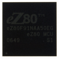
EZ80F91NAA50EG Zilog, EZ80F91NAA50EG Datasheet - Page 280

EZ80F91NAA50EG
Manufacturer Part Number
EZ80F91NAA50EG
Description
IC ACCLAIM MCU 256KB 144BGA
Manufacturer
Zilog
Series
eZ80® AcclaimPlus!™r
Datasheet
1.EZ80F91AZA50SG.pdf
(387 pages)
Specifications of EZ80F91NAA50EG
Core Processor
Z8
Core Size
8-Bit
Speed
50MHz
Connectivity
Ethernet, I²C, IrDA, SPI, UART/USART
Peripherals
Brown-out Detect/Reset, POR, PWM, WDT
Number Of I /o
32
Program Memory Size
256KB (256K x 8)
Program Memory Type
FLASH
Ram Size
16K x 8
Voltage - Supply (vcc/vdd)
3 V ~ 3.6 V
Oscillator Type
Internal
Operating Temperature
-40°C ~ 105°C
Package / Case
144-LBGA
Processor Series
EZ80F91x
Core
eZ80
Data Bus Width
8 bit
Data Ram Size
8 KB
Interface Type
I2C, IrDA, SPI
Maximum Clock Frequency
50 MHz
Number Of Programmable I/os
32
Number Of Timers
4
Operating Supply Voltage
3 V to 3.6 V
Maximum Operating Temperature
+ 105 C
Mounting Style
SMD/SMT
Development Tools By Supplier
eZ80F910300ZCOG, eZ80F910200KITG
Minimum Operating Temperature
- 40 C
For Use With
269-4712 - KIT DEV ENCORE 32 SERIES269-4671 - BOARD ZDOTS SBC Z80ACCLAIM PLUS269-4561 - KIT DEV FOR EZ80F91 W/C-COMPILER269-4560 - KIT DEV FOR EZ80F91 W/C-COMPILER
Lead Free Status / RoHS Status
Lead free / RoHS Compliant
Eeprom Size
-
Data Converters
-
Lead Free Status / Rohs Status
Details
Other names
269-4565
Available stocks
Company
Part Number
Manufacturer
Quantity
Price
- Current page: 280 of 387
- Download datasheet (5Mb)
Table 152. PLL Divider Register—Low Bytes
PS027001-0707
Bit
Reset
CPU Access
Note: W = Write only.
Bit
Position
[7:0]
PLL_DIV_L
Note:
Power Requirement to the Phase-Locked Loop Function
PLL Registers
Regardless of whether or not you chooses to use the PLL module block as a clock source
for the eZ80F91 device, the PLL_V
the PLL_V
eZ80F91 using any system clock source.
PLL Divider Control Register—Low and High Bytes
This register is designed such that the 11 bit divider value is loaded into the divider mod-
ule whenever the PLL_DIV_H register is written. Therefore, the procedure must be to
load the PLL_DIV_L register, followed by the PLL_DIV_H register, for the divider to
receive the appropriate value.
The divider is designed such that any divider value less than two is ignored; a value of two
is used in its place.
The least-significant byte of PLL divider N is set via the corresponding bits in the
PLL_DIV_L register. See
The PLL divider register are written only when the PLL is disabled. A read-back of the
PLL Divider registers returns 0.
Value
00h–FFh These bits represent the Low byte of the 11 bit PLL divider
SS
W
7
0
Description
value. The complete PLL divider value is returned by
{PLL_DIV_H, PLL_DIV_L}.
(pin 84) must be connected to a V
W
6
0
Table 152
W
5
0
DD
W
4
0
(PLL_DIV_L = 005Ch)
and
(pin 87) must be connected to a V
Table 153
W
3
0
SS
supply for proper operation of the
on page 273.
W
2
0
W
1
1
Product Specification
W
0
0
Phase-Locked Loop
eZ80F91 ASSP
DD
supply and
272
Related parts for EZ80F91NAA50EG
Image
Part Number
Description
Manufacturer
Datasheet
Request
R

Part Number:
Description:
Communication Controllers, ZILOG INTELLIGENT PERIPHERAL CONTROLLER (ZIP)
Manufacturer:
Zilog, Inc.
Datasheet:

Part Number:
Description:
KIT DEV FOR Z8 ENCORE 16K TO 64K
Manufacturer:
Zilog
Datasheet:

Part Number:
Description:
KIT DEV Z8 ENCORE XP 28-PIN
Manufacturer:
Zilog
Datasheet:

Part Number:
Description:
DEV KIT FOR Z8 ENCORE 8K/4K
Manufacturer:
Zilog
Datasheet:

Part Number:
Description:
KIT DEV Z8 ENCORE XP 28-PIN
Manufacturer:
Zilog
Datasheet:

Part Number:
Description:
DEV KIT FOR Z8 ENCORE 4K TO 8K
Manufacturer:
Zilog
Datasheet:

Part Number:
Description:
CMOS Z8 microcontroller. ROM 16 Kbytes, RAM 256 bytes, speed 16 MHz, 32 lines I/O, 3.0V to 5.5V
Manufacturer:
Zilog, Inc.
Datasheet:

Part Number:
Description:
Low-cost microcontroller. 512 bytes ROM, 61 bytes RAM, 8 MHz
Manufacturer:
Zilog, Inc.
Datasheet:

Part Number:
Description:
Z8 4K OTP Microcontroller
Manufacturer:
Zilog, Inc.
Datasheet:

Part Number:
Description:
CMOS SUPER8 ROMLESS MCU
Manufacturer:
Zilog, Inc.
Datasheet:

Part Number:
Description:
SL1866 CMOSZ8 OTP Microcontroller
Manufacturer:
Zilog, Inc.
Datasheet:

Part Number:
Description:
SL1866 CMOSZ8 OTP Microcontroller
Manufacturer:
Zilog, Inc.
Datasheet:

Part Number:
Description:
OTP (KB) = 1, RAM = 125, Speed = 12, I/O = 14, 8-bit Timers = 2, Comm Interfaces Other Features = Por, LV Protect, Voltage = 4.5-5.5V
Manufacturer:
Zilog, Inc.
Datasheet:

Part Number:
Description:
Manufacturer:
Zilog, Inc.
Datasheet:


