MC908JB16DWE Freescale Semiconductor, MC908JB16DWE Datasheet - Page 250
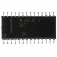
MC908JB16DWE
Manufacturer Part Number
MC908JB16DWE
Description
IC MCU 16K FLASH 6MHZ USB 28SOIC
Manufacturer
Freescale Semiconductor
Series
HC08r
Specifications of MC908JB16DWE
Core Processor
HC08
Core Size
8-Bit
Speed
6MHz
Connectivity
SCI, USB
Peripherals
LED, LVD, POR, PWM
Number Of I /o
21
Program Memory Size
16KB (16K x 8)
Program Memory Type
FLASH
Ram Size
384 x 8
Voltage - Supply (vcc/vdd)
4 V ~ 5.5 V
Oscillator Type
Internal
Operating Temperature
0°C ~ 70°C
Package / Case
28-SOIC (7.5mm Width)
Processor Series
HC08JB
Core
HC08
Data Bus Width
8 bit
Data Ram Size
384 B
Interface Type
I2C/SCI/SPI/USB
Maximum Clock Frequency
12 MHz
Number Of Programmable I/os
21
Number Of Timers
4
Operating Supply Voltage
5.5 V
Maximum Operating Temperature
+ 70 C
Mounting Style
SMD/SMT
Development Tools By Supplier
FSICEBASE, DEMO908GZ60E, M68EML08GZE, KITUSBSPIDGLEVME, KITUSBSPIEVME, KIT33810EKEVME
Minimum Operating Temperature
0 C
Controller Family/series
HC08
No. Of I/o's
21
Ram Memory Size
384Byte
Cpu Speed
8MHz
No. Of Timers
2
Embedded Interface Type
I2C, SCI, SPI
Rohs Compliant
Yes
Lead Free Status / RoHS Status
Lead free / RoHS Compliant
Eeprom Size
-
Data Converters
-
Lead Free Status / Rohs Status
Lead free / RoHS Compliant
Available stocks
Company
Part Number
Manufacturer
Quantity
Price
Company:

Part Number:
MC908JB16DWE
Manufacturer:
FREESCALE
Quantity:
1 831
Part Number:
MC908JB16DWE
Manufacturer:
FRE/MOT
Quantity:
20 000


Clock Generator Module (CGM)
13.3.1 Reference Frequency Source (OSCXCLK)
13.3.2 Voltage Controlled Oscillator
Technical Data
250
OSCXCLK
REFERENCE
DIVIDER
RDS[9:0]
R
CGMRCLK
The OSCXCLK signal is a buffered output of the crystal oscillator circuit
and runs at a rate equal to the crystal frequency. OSCXCLK is used as
the reference frequency source for both CGM modules.
The VCO clock frequency (CGMVCLK) is generated internally and it is
proportional to the controlled voltage setting by the phase detector
output. The VCO operating range is programmable for a wide range of
frequencies and for maximum immunity to external noise. The
CGMVCLK signal is also the CGM output signal, CGMOUT.
Figure 13-2. CGM Block Diagram
Clock Generator Module (CGM)
DETECTOR
DETECTOR
CGMFCLK
PHD_[7:0]
PHASE
LOCK
LOCK
V
DDA
VDS[11:0]
CGMXFC
DIVIDER
FILTER
LOOP
VCO
N
PLL ANALOG
V
SSA
PLLON
CONTROLLED
OSCILLATOR
CGMVCLK
VOLTAGE
V
MC68HC908JB16
REGA
Freescale Semiconductor
VCO_[7:0]
—
CGMOUT
Rev. 1.1
Related parts for MC908JB16DWE
Image
Part Number
Description
Manufacturer
Datasheet
Request
R

Part Number:
Description:
Manufacturer:
Freescale Semiconductor, Inc
Datasheet:
Part Number:
Description:
Manufacturer:
Freescale Semiconductor, Inc
Datasheet:
Part Number:
Description:
Manufacturer:
Freescale Semiconductor, Inc
Datasheet:
Part Number:
Description:
Manufacturer:
Freescale Semiconductor, Inc
Datasheet:
Part Number:
Description:
Manufacturer:
Freescale Semiconductor, Inc
Datasheet:
Part Number:
Description:
Manufacturer:
Freescale Semiconductor, Inc
Datasheet:
Part Number:
Description:
Manufacturer:
Freescale Semiconductor, Inc
Datasheet:
Part Number:
Description:
Manufacturer:
Freescale Semiconductor, Inc
Datasheet:
Part Number:
Description:
Manufacturer:
Freescale Semiconductor, Inc
Datasheet:
Part Number:
Description:
Manufacturer:
Freescale Semiconductor, Inc
Datasheet:
Part Number:
Description:
Manufacturer:
Freescale Semiconductor, Inc
Datasheet:
Part Number:
Description:
Manufacturer:
Freescale Semiconductor, Inc
Datasheet:
Part Number:
Description:
Manufacturer:
Freescale Semiconductor, Inc
Datasheet:
Part Number:
Description:
Manufacturer:
Freescale Semiconductor, Inc
Datasheet:
Part Number:
Description:
Manufacturer:
Freescale Semiconductor, Inc
Datasheet: