MC908JB16DWE Freescale Semiconductor, MC908JB16DWE Datasheet - Page 276
MC908JB16DWE
Manufacturer Part Number
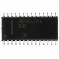
MC908JB16DWE
Description
IC MCU 16K FLASH 6MHZ USB 28SOIC
Manufacturer
Freescale Semiconductor
Series
HC08r
Specifications of MC908JB16DWE
Core Processor
HC08
Core Size
8-Bit
Speed
6MHz
Connectivity
SCI, USB
Peripherals
LED, LVD, POR, PWM
Number Of I /o
21
Program Memory Size
16KB (16K x 8)
Program Memory Type
FLASH
Ram Size
384 x 8
Voltage - Supply (vcc/vdd)
4 V ~ 5.5 V
Oscillator Type
Internal
Operating Temperature
0°C ~ 70°C
Package / Case
28-SOIC (7.5mm Width)
Processor Series
HC08JB
Core
HC08
Data Bus Width
8 bit
Data Ram Size
384 B
Interface Type
I2C/SCI/SPI/USB
Maximum Clock Frequency
12 MHz
Number Of Programmable I/os
21
Number Of Timers
4
Operating Supply Voltage
5.5 V
Maximum Operating Temperature
+ 70 C
Mounting Style
SMD/SMT
Development Tools By Supplier
FSICEBASE, DEMO908GZ60E, M68EML08GZE, KITUSBSPIDGLEVME, KITUSBSPIEVME, KIT33810EKEVME
Minimum Operating Temperature
0 C
Controller Family/series
HC08
No. Of I/o's
21
Ram Memory Size
384Byte
Cpu Speed
8MHz
No. Of Timers
2
Embedded Interface Type
I2C, SCI, SPI
Rohs Compliant
Yes
Lead Free Status / RoHS Status
Lead free / RoHS Compliant
Eeprom Size
-
Data Converters
-
Lead Free Status / Rohs Status
Lead free / RoHS Compliant
Available stocks
Company
Part Number
Manufacturer
Quantity
Price
Company:

Part Number:
MC908JB16DWE
Manufacturer:
FREESCALE
Quantity:
1 831
Part Number:
MC908JB16DWE
Manufacturer:
FRE/MOT
Quantity:
20 000


Input/Output (I/O) Ports
Technical Data
276
NOTE:
D– and D+ — USB Data Pins
PTE4/D– pin has two programmable pullup resistors. One is used for
PTE4 when the USB module is disabled and another is used for D–
when the USB module is enabled.
T2CH01 and T1CH01 — Timer Channel I/O Bits
TCLK — Timer Clock Input
The PTE[2:0] pullup enable bit, PTE20P, in the port option control
register (POCR) enables pullups on PTE2–PTE0, regardless of the
pin is configured as an input or an output. (See
PTE4 pin functions as an external interrupt when PTE4IE=1 in the
IRQ option control register (IOCR) and USBEN=0 in the USB address
register (USB disabled). (See
D– and D+ are the differential data lines used by the USB module.
(See
The USB module enable bit, USBEN, in the USB address register
(UADDR) controls the pin options for PTE4/D– and PTE3/D+. When
the USB module is enabled, PTE4/D– and PTE3/D+ function as USB
data pins D– and D+. When the USB module is disabled, PTE4/D–
and PTE3/D+ function as 10mA open-drain high current pins for PS/2
clock and data use.
The pullup enable bit, PULLEN, in the USB control register 3 (UCR3)
enables a 1.5kΩ pullup on D– pin when the USB module is enabled.
(See
The PTE2/T2CH01 and PTE1/T1CH01 pins are the respective TIM2
and TIM1 input capture/output compare pins. The edge/level select
bits, ELSxB and ELSxA, determine whether the PTE2/T2CH01 and
PTE1/T1CH01 pins are timer channel I/O pins or general-purpose I/O
pins. (See
The PTE0/TCLK pin is the external clock input for TIM1 and TIM2.
The prescaler select bits, PS[2:0], select PTE0/TCLK as the TIM
clock input. When not selected as the TIM clock, PTE0/TCLK is
available for general purpose I/O. (See
Module
Section 11. Universal Serial Bus Module
11.8.8 USB Control Register
(TIM).)
Section 10. Timer Interface Module
Input/Output (I/O) Ports
15.9 IRQ Option Control
3.)
Section 10. Timer Interface
MC68HC908JB16
Freescale Semiconductor
14.7 Port
(TIM).)
(USB).)
Register.)
Options.)
—
Rev. 1.1
Related parts for MC908JB16DWE
Image
Part Number
Description
Manufacturer
Datasheet
Request
R

Part Number:
Description:
Manufacturer:
Freescale Semiconductor, Inc
Datasheet:
Part Number:
Description:
Manufacturer:
Freescale Semiconductor, Inc
Datasheet:
Part Number:
Description:
Manufacturer:
Freescale Semiconductor, Inc
Datasheet:
Part Number:
Description:
Manufacturer:
Freescale Semiconductor, Inc
Datasheet:
Part Number:
Description:
Manufacturer:
Freescale Semiconductor, Inc
Datasheet:
Part Number:
Description:
Manufacturer:
Freescale Semiconductor, Inc
Datasheet:
Part Number:
Description:
Manufacturer:
Freescale Semiconductor, Inc
Datasheet:
Part Number:
Description:
Manufacturer:
Freescale Semiconductor, Inc
Datasheet:
Part Number:
Description:
Manufacturer:
Freescale Semiconductor, Inc
Datasheet:
Part Number:
Description:
Manufacturer:
Freescale Semiconductor, Inc
Datasheet:
Part Number:
Description:
Manufacturer:
Freescale Semiconductor, Inc
Datasheet:
Part Number:
Description:
Manufacturer:
Freescale Semiconductor, Inc
Datasheet:
Part Number:
Description:
Manufacturer:
Freescale Semiconductor, Inc
Datasheet:
Part Number:
Description:
Manufacturer:
Freescale Semiconductor, Inc
Datasheet:
Part Number:
Description:
Manufacturer:
Freescale Semiconductor, Inc
Datasheet: