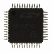
C8051F360-GQ Silicon Laboratories Inc, C8051F360-GQ Datasheet - Page 72

C8051F360-GQ
Manufacturer Part Number
C8051F360-GQ
Description
IC 8051 MCU 32K FLASH 48TQFP
Manufacturer
Silicon Laboratories Inc
Series
C8051F36xr
Specifications of C8051F360-GQ
Program Memory Type
FLASH
Program Memory Size
32KB (32K x 8)
Package / Case
48-TQFP, 48-VQFP
Core Processor
8051
Core Size
8-Bit
Speed
100MHz
Connectivity
EBI/EMI, SMBus (2-Wire/I²C), SPI, UART/USART
Peripherals
POR, PWM, Temp Sensor, WDT
Number Of I /o
39
Ram Size
1K x 8
Voltage - Supply (vcc/vdd)
3 V ~ 3.6 V
Data Converters
A/D 17x10b; D/A 1x10b
Oscillator Type
Internal
Operating Temperature
-40°C ~ 85°C
Processor Series
C8051F3x
Core
8051
Data Bus Width
8 bit
Data Ram Size
1 KB
Interface Type
I2C/SMBus/SPI/UART
Maximum Clock Frequency
100 MHz
Number Of Programmable I/os
39
Number Of Timers
4
Operating Supply Voltage
3 V to 3.6 V
Maximum Operating Temperature
+ 85 C
Mounting Style
SMD/SMT
3rd Party Development Tools
KSK-SL-TOOLSTICK, PK51, CA51, A51, ULINK2
Development Tools By Supplier
C8051F360DK
Minimum Operating Temperature
- 40 C
On-chip Adc
21-ch x 10-bit
On-chip Dac
1-ch x 10-bit
Package
48TQFP
Device Core
8051
Family Name
C8051F36x
Maximum Speed
100 MHz
Lead Free Status / RoHS Status
Lead free / RoHS Compliant
For Use With
336-1483 - ADAPTER PROGRAM TOOLSTICK F360770-1006 - ISP 4PORT FOR SILABS C8051F MCU336-1412 - BOARD TARGET/PROTO W/C8051F360336-1411 - DAUGHTER CARD TOOLSTCK C8051F362336-1410 - KIT DEV FOR C8051F360 FAMILY
Eeprom Size
-
Lead Free Status / Rohs Status
Lead free / RoHS Compliant
Other names
336-1407
Available stocks
Company
Part Number
Manufacturer
Quantity
Price
Company:
Part Number:
C8051F360-GQ
Manufacturer:
Silicon Laboratories Inc
Quantity:
10 000
Part Number:
C8051F360-GQ
Manufacturer:
SILICON LABS/èٹ¯ç§‘
Quantity:
20 000
Company:
Part Number:
C8051F360-GQR
Manufacturer:
Silicon Laboratories Inc
Quantity:
10 000
Part Number:
C8051F360-GQR
Manufacturer:
SILICON LABS/èٹ¯ç§‘
Quantity:
20 000
C8051F360/1/2/3/4/5/6/7/8/9
The Comparator hysteresis is software-programmable via the Comparator Control registers CPT0CN and
CPT1CN. The user can program both the amount of hysteresis voltage (referred to the input voltage) and
the positive and negative-going symmetry of this hysteresis around the threshold voltage.
The Comparator hysteresis is programmed using Bits3–0 in the Comparator Control registers CPT0CN
and CPT1CN (shown in SFR Definition 8.1 and SFR Definition 8.4). The amount of negative hysteresis
voltage is determined by the settings of the CP0HYN and CP1HYN bits. As shown in Figure 8.3, settings of
20, 10 or 5 mV of negative hysteresis can be programmed, or negative hysteresis can be disabled. In a
similar way, the amount of positive hysteresis is determined by the setting the CP0HYP and CP1HYP bits.
Comparator interrupts can be generated on both rising-edge and falling-edge output transitions. (For Inter-
rupt enable and priority control, see Section “10. Interrupt Handler” on page 107). The CP0FIF or CP1FIF
flag is set to logic ‘1’ upon a Comparator falling-edge occurrence, and the CP0RIF or CP1RIF flag is set to
logic ‘1’ upon the Comparator rising-edge occurrence. Once set, these bits remain set until cleared by soft-
ware. The Comparator rising-edge interrupt mask is enabled by setting CP0RIE or CP1RIE to a logic ‘1’.
The Comparator falling-edge interrupt mask is enabled by setting CP0FIE or CP1FIE to a logic ‘1’.
The output state of the Comparator can be obtained at any time by reading the CP0OUT or CP1OUT bit.
The Comparator is enabled by setting the CP0EN or CP1EN bit to logic ‘1’, and is disabled by clearing this
bit to logic ‘0’.
Note that false rising edges and falling edges can be detected when the comparator is first powered on or
if changes are made to the hysteresis or response time control bits. Therefore, it is recommended that the
rising-edge and falling-edge flags be explicitly cleared to logic ‘0’ a short time after the comparator is
enabled or its mode bits have been changed. This Power Up Time is specified in Table 8.1 on page 79.
72
(Programmed with CP0HYP Bits)
Positive Hysteresis Voltage
INPUTS
OUTPUT
VIN+
VIN-
CIRCUIT CONFIGURATION
Positive Hysteresis
CP0-
CP0+
VIN+
VIN-
Disabled
V
OL
Figure 8.3. Comparator Hysteresis Plot
V
OH
+
_
CP0
Positive Hysteresis
Maximum
OUT
Rev. 1.0
Negative Hysteresis
Disabled
Negative Hysteresis
(Programmed by CP0HYN Bits)
Maximum
Negative Hysteresis Voltage


