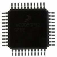
MC908GP32CFBE Freescale Semiconductor, MC908GP32CFBE Datasheet - Page 43

MC908GP32CFBE
Manufacturer Part Number
MC908GP32CFBE
Description
IC MCU 8MHZ 32K FLASH 44-QFP
Manufacturer
Freescale Semiconductor
Series
HC08r
Datasheet
1.MC908GP32CFBE.pdf
(266 pages)
Specifications of MC908GP32CFBE
Core Processor
HC08
Core Size
8-Bit
Speed
8MHz
Connectivity
SCI, SPI
Peripherals
LVD, POR, PWM
Number Of I /o
33
Program Memory Size
32KB (32K x 8)
Program Memory Type
FLASH
Ram Size
512 x 8
Voltage - Supply (vcc/vdd)
2.7 V ~ 5.5 V
Data Converters
A/D 8x8b
Oscillator Type
Internal
Operating Temperature
-40°C ~ 85°C
Package / Case
44-QFP
Processor Series
HC08GP
Core
HC08
Data Bus Width
8 bit
Data Ram Size
512 B
Interface Type
SCI, SPI
Maximum Clock Frequency
8 MHz
Number Of Programmable I/os
33
Number Of Timers
4
Maximum Operating Temperature
+ 85 C
Mounting Style
SMD/SMT
Development Tools By Supplier
FSICEBASE, DEMO908GZ60E, M68CBL05CE, M68EML08GPGTE
Minimum Operating Temperature
- 40 C
On-chip Adc
8 bit, 8 Channel
Lead Free Status / RoHS Status
Lead free / RoHS Compliant
Eeprom Size
-
Lead Free Status / Rohs Status
Details
Available stocks
Company
Part Number
Manufacturer
Quantity
Price
Company:
Part Number:
MC908GP32CFBE
Manufacturer:
WAVEFRONT
Quantity:
9 183
Company:
Part Number:
MC908GP32CFBE
Manufacturer:
FREESCALE
Quantity:
5 530
Company:
Part Number:
MC908GP32CFBE
Manufacturer:
FREE
Quantity:
4
Company:
Part Number:
MC908GP32CFBE
Manufacturer:
Freescale Semiconductor
Quantity:
10 000
Part Number:
MC908GP32CFBE
Manufacturer:
FREESCALE
Quantity:
20 000
Company:
Part Number:
MC908GP32CFBER
Manufacturer:
Freescale Semiconductor
Quantity:
10 000
Freescale Semiconductor
Algorithm for programming
a row (64 bytes) of FLASH memory
NOTE:
The time between each FLASH address change (step 7 to step 7), or
the time between the last FLASH address programmed
to clearing PGM bit (step 7 to step 10)
must not exceed the maximum programming
time, t
This row program algorithm assumes the row/s
to be programmed are initially erased.
PROG
max.
Figure 2-4. FLASH Programming Flowchart
MC68HC908GP32 Data Sheet, Rev. 10
1
2
3
4
5
6
7
8
Read the FLASH block protect register
Write any data to any FLASH address
within the row address range desired
Write data to the FLASH address
to be programmed
Wait for a time, t
Wait for a time, t
Wait for a time, t
Set HVEN bit
programming
Set PGM bit
Completed
this row?
N
PROG
pgs
nvs
10
11
12
13
Y
End of programming
Wait for a time, t
Wait for a time, t
Clear HVEN bit
Clear PGM bit
nvh
rcv
FLASH Memory
43


