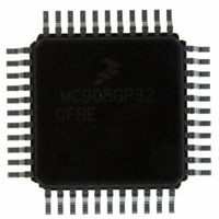
MC908GP32CFBE Freescale Semiconductor, MC908GP32CFBE Datasheet - Page 44

MC908GP32CFBE
Manufacturer Part Number
MC908GP32CFBE
Description
IC MCU 8MHZ 32K FLASH 44-QFP
Manufacturer
Freescale Semiconductor
Series
HC08r
Datasheet
1.MC908GP32CFBE.pdf
(266 pages)
Specifications of MC908GP32CFBE
Core Processor
HC08
Core Size
8-Bit
Speed
8MHz
Connectivity
SCI, SPI
Peripherals
LVD, POR, PWM
Number Of I /o
33
Program Memory Size
32KB (32K x 8)
Program Memory Type
FLASH
Ram Size
512 x 8
Voltage - Supply (vcc/vdd)
2.7 V ~ 5.5 V
Data Converters
A/D 8x8b
Oscillator Type
Internal
Operating Temperature
-40°C ~ 85°C
Package / Case
44-QFP
Processor Series
HC08GP
Core
HC08
Data Bus Width
8 bit
Data Ram Size
512 B
Interface Type
SCI, SPI
Maximum Clock Frequency
8 MHz
Number Of Programmable I/os
33
Number Of Timers
4
Maximum Operating Temperature
+ 85 C
Mounting Style
SMD/SMT
Development Tools By Supplier
FSICEBASE, DEMO908GZ60E, M68CBL05CE, M68EML08GPGTE
Minimum Operating Temperature
- 40 C
On-chip Adc
8 bit, 8 Channel
Lead Free Status / RoHS Status
Lead free / RoHS Compliant
Eeprom Size
-
Lead Free Status / Rohs Status
Details
Available stocks
Company
Part Number
Manufacturer
Quantity
Price
Company:
Part Number:
MC908GP32CFBE
Manufacturer:
WAVEFRONT
Quantity:
9 183
Company:
Part Number:
MC908GP32CFBE
Manufacturer:
FREESCALE
Quantity:
5 530
Company:
Part Number:
MC908GP32CFBE
Manufacturer:
FREE
Quantity:
4
Company:
Part Number:
MC908GP32CFBE
Manufacturer:
Freescale Semiconductor
Quantity:
10 000
Part Number:
MC908GP32CFBE
Manufacturer:
FREESCALE
Quantity:
20 000
Company:
Part Number:
MC908GP32CFBER
Manufacturer:
Freescale Semiconductor
Quantity:
10 000
Memory
When the FLBPR is programmed with all 0’s, the entire memory is protected from being programmed and
erased. When all the bits are erased (all 1’s), the entire memory is accessible for program and erase.
When bits within the FLBPR are programmed, they lock a block of memory, address ranges as shown in
2.6.6.1 FLASH Block Protect
erase or program of the FLBPR or the protected block of FLASH memory is prohibited. Mass erase is
disabled whenever any block is protected (FLBPR does not equal $FF). The presence of a V
IRQ pin will bypass the block protection so that all of the memory included in the block protect register is
open for program and erase operations.
2.6.6.1 FLASH Block Protect Register
The FLASH block protect register (FLBPR) is implemented as a byte within the FLASH memory, and
therefore can only be written during a programming sequence of the FLASH memory. The value in this
register determines the starting location of the protected range within the FLASH memory.
BPR[7:0] — FLASH Block Protect Bits
44
These eight bits represent bits [14:7] of a 16-bit memory address.
Bit-15 is 1 and bits [6:0] are 0s.
The resultant 16-bit address is used for specifying the start address of the FLASH memory for block
protection. The FLASH is protected from this start address to the end of FLASH memory, at $FFFF.
With this mechanism, the protect start address can be XX00 and XX80 (128 bytes page boundaries)
within the FLASH memory.
Address:
The FLASH block protect register is not protected with special hardware or
software. Therefore, if this page is not protected by FLBPR the register is
erased by either a page or mass erase operation.
Reset:
Read:
Write:
Start address of FLASH block protect
U = Unaffected by reset. Initial value from factory is 1.
Write to this register is by a programming sequence to the FLASH memory.
$FF7E
BPR7
Bit 7
U
Figure 2-5. FLASH Block Protect Register (FLBPR)
Figure 2-6. FLASH Block Protect Start Address
Register. Once the FLBPR is programmed with a value other than $FF, any
BPR6
U
6
MC68HC908GP32 Data Sheet, Rev. 10
BPR5
U
5
1
NOTE
BPR4
U
4
FLBPR value
16-bit memory address
BPR3
U
3
BPR2
0 0 0 0 0 0 0
U
2
BPR1
U
1
Freescale Semiconductor
BPR0
Bit 0
U
TST
on the


