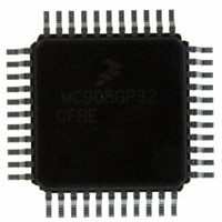
MC908GP32CFBE Freescale Semiconductor, MC908GP32CFBE Datasheet - Page 81

MC908GP32CFBE
Manufacturer Part Number
MC908GP32CFBE
Description
IC MCU 8MHZ 32K FLASH 44-QFP
Manufacturer
Freescale Semiconductor
Series
HC08r
Datasheet
1.MC908GP32CFBE.pdf
(266 pages)
Specifications of MC908GP32CFBE
Core Processor
HC08
Core Size
8-Bit
Speed
8MHz
Connectivity
SCI, SPI
Peripherals
LVD, POR, PWM
Number Of I /o
33
Program Memory Size
32KB (32K x 8)
Program Memory Type
FLASH
Ram Size
512 x 8
Voltage - Supply (vcc/vdd)
2.7 V ~ 5.5 V
Data Converters
A/D 8x8b
Oscillator Type
Internal
Operating Temperature
-40°C ~ 85°C
Package / Case
44-QFP
Processor Series
HC08GP
Core
HC08
Data Bus Width
8 bit
Data Ram Size
512 B
Interface Type
SCI, SPI
Maximum Clock Frequency
8 MHz
Number Of Programmable I/os
33
Number Of Timers
4
Maximum Operating Temperature
+ 85 C
Mounting Style
SMD/SMT
Development Tools By Supplier
FSICEBASE, DEMO908GZ60E, M68CBL05CE, M68EML08GPGTE
Minimum Operating Temperature
- 40 C
On-chip Adc
8 bit, 8 Channel
Lead Free Status / RoHS Status
Lead free / RoHS Compliant
Eeprom Size
-
Lead Free Status / Rohs Status
Details
Available stocks
Company
Part Number
Manufacturer
Quantity
Price
Company:
Part Number:
MC908GP32CFBE
Manufacturer:
WAVEFRONT
Quantity:
9 183
Company:
Part Number:
MC908GP32CFBE
Manufacturer:
FREESCALE
Quantity:
5 530
Company:
Part Number:
MC908GP32CFBE
Manufacturer:
FREE
Quantity:
4
Company:
Part Number:
MC908GP32CFBE
Manufacturer:
Freescale Semiconductor
Quantity:
10 000
Part Number:
MC908GP32CFBE
Manufacturer:
FREESCALE
Quantity:
20 000
Company:
Part Number:
MC908GP32CFBER
Manufacturer:
Freescale Semiconductor
Quantity:
10 000
Chapter 6
Configuration Register (CONFIG)
6.1 Introduction
This section describes the configuration registers, CONFIG1 and CONFIG2. The configuration registers
enable or disable these options:
6.2 Functional Description
The configuration registers are used in the initialization of various options. The configuration registers can
be written once after each reset. All of the configuration register bits are cleared during reset. Since the
various options affect the operation of the MCU, it is recommended that these registers be written
immediately after reset. The configuration registers are located at $001E and $001F. The configuration
register may be read at anytime.
Freescale Semiconductor
•
•
•
•
•
•
Stop mode recovery time (32 CGMXCLK cycles or 4096 CGMXCLK cycles)
COP timeout period (262,128 or 8176 CGMXCLK cycles)
STOP instruction
Computer operating properly module (COP)
Low-voltage inhibit (LVI) module control and voltage trip point selection
Enable/disable the oscillator (OSC) during stop mode
Address:
Reset:
On a FLASH device, the options except LVI5OR3 are one-time writeable
by the user after each reset. The LVI5OR3 bit is one-time writeable by the
user only after each POR (power-on reset). The CONFIG registers are not
in the FLASH memory but are special registers containing one-time
writeable latches after each reset. Upon a reset, the CONFIG registers
default to predetermined settings as shown in
Read:
Write:
Bit 7
$001E
0
0
Figure 6-1. Configuration Register 2 (CONFIG2)
= Unimplemented
6
0
0
MC68HC908GP32 Data Sheet, Rev. 10
5
0
0
NOTE
4
0
0
3
0
0
Figure 6-1
2
0
0
and
OSCSTOPENB SCIBDSRC
Figure
1
0
6-2.
Bit 0
0
81


