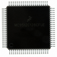
MC9S12C128CFUE Freescale Semiconductor, MC9S12C128CFUE Datasheet - Page 152

MC9S12C128CFUE
Manufacturer Part Number
MC9S12C128CFUE
Description
IC MCU 128K FLASH 25MHZ 80-QFP
Manufacturer
Freescale Semiconductor
Series
HCS12r
Specifications of MC9S12C128CFUE
Core Processor
HCS12
Core Size
16-Bit
Speed
25MHz
Connectivity
CAN, EBI/EMI, SCI, SPI
Peripherals
POR, PWM, WDT
Number Of I /o
60
Program Memory Size
128KB (128K x 8)
Program Memory Type
FLASH
Ram Size
4K x 8
Voltage - Supply (vcc/vdd)
2.35 V ~ 5.5 V
Data Converters
A/D 8x10b
Oscillator Type
Internal
Operating Temperature
-40°C ~ 85°C
Package / Case
80-QFP
Cpu Family
HCS12
Device Core Size
16b
Frequency (max)
25MHz
Interface Type
CAN/SCI/SPI
Total Internal Ram Size
4KB
# I/os (max)
60
Number Of Timers - General Purpose
8
Operating Supply Voltage (typ)
2.5/5V
Operating Supply Voltage (max)
2.75/5.5V
Operating Supply Voltage (min)
2.35/2.97V
On-chip Adc
8-chx10-bit
Instruction Set Architecture
CISC
Operating Temp Range
-40C to 85C
Operating Temperature Classification
Industrial
Mounting
Surface Mount
Pin Count
80
Package Type
PQFP
Processor Series
S12C
Core
HCS12
Data Bus Width
16 bit
Data Ram Size
4000 B
Maximum Clock Frequency
25 MHz
Number Of Programmable I/os
61
Number Of Timers
1
Operating Supply Voltage
- 0.3 V to + 6.5 V
Maximum Operating Temperature
+ 85 C
Mounting Style
SMD/SMT
3rd Party Development Tools
EWHCS12
Development Tools By Supplier
M68EVB912C32EE
Minimum Operating Temperature
- 40 C
Lead Free Status / RoHS Status
Lead free / RoHS Compliant
Eeprom Size
-
Lead Free Status / Rohs Status
Compliant
Available stocks
Company
Part Number
Manufacturer
Quantity
Price
Company:
Part Number:
MC9S12C128CFUE
Manufacturer:
ST
Quantity:
6 246
Company:
Part Number:
MC9S12C128CFUE
Manufacturer:
Freescale Semiconductor
Quantity:
10 000
- Current page: 152 of 690
- Download datasheet (4Mb)
Chapter 4 Multiplexed External Bus Interface (MEBIV3)
There are two basic types of operating modes:
A system development and debug feature, background debug mode (BDM), is available in all modes. In
special single-chip mode, BDM is active immediately after reset.
Some aspects of Port E are not mode dependent. Bit 1 of Port E is a general purpose input or the IRQ
interrupt input. IRQ can be enabled by bits in the CPU’s condition codes register but it is inhibited at reset
so this pin is initially configured as a simple input with a pull-up. Bit 0 of Port E is a general purpose input
or the XIRQ interrupt input. XIRQ can be enabled by bits in the CPU’s condition codes register but it is
inhibited at reset so this pin is initially configured as a simple input with a pull-up. The ESTR bit in the
EBICTL register is set to one by reset in any user mode. This assures that the reset vector can be fetched
even if it is located in an external slow memory device. The PE6/MODB/IPIPE1 and PE5/MODA/IPIPE0
pins act as high-impedance mode select inputs during reset.
The following paragraphs discuss the default bus setup and describe which aspects of the bus can be
changed after reset on a per mode basis.
4.4.3.1
These modes provide three operating configurations. Background debug is available in all three modes, but
must first be enabled for some operations by means of a BDM background command, then activated.
4.4.3.1.1
There is no external expansion bus in this mode. All pins of Ports A, B and E are configured as general
purpose I/O pins Port E bits 1 and 0 are available as general purpose input only pins with internal pull
resistors enabled. All other pins of Port E are bidirectional I/O pins that are initially configured as high-
impedance inputs with internal pull resistors enabled. Ports A and B are configured as high-impedance
inputs with their internal pull resistors disabled.
The pins associated with Port E bits 6, 5, 3, and 2 cannot be configured for their alternate functions IPIPE1,
IPIPE0, LSTRB, and R/W while the MCU is in single chip modes. In single chip modes, the associated
control bits PIPOE, LSTRE, and RDWE are reset to zero. Writing the opposite state into them in single
chip mode does not change the operation of the associated Port E pins.
In normal single chip mode, the MODE register is writable one time. This allows a user program to change
the bus mode to narrow or wide expanded mode and/or turn on visibility of internal accesses.
Port E, bit 4 can be configured for a free-running E clock output by clearing NECLK=0. Typically the only
use for an E clock output while the MCU is in single chip modes would be to get a constant speed clock
for use in the external application system.
152
1. Normal modes: Some registers and bits are protected against accidental changes.
2. Special modes: Allow greater access to protected control registers and bits for special purposes
such as testing.
Normal Operating Modes
Normal Single-Chip Mode
MC9S12C-Family / MC9S12GC-Family
Rev 01.24
Freescale Semiconductor
Related parts for MC9S12C128CFUE
Image
Part Number
Description
Manufacturer
Datasheet
Request
R
Part Number:
Description:
Manufacturer:
Freescale Semiconductor, Inc
Datasheet:
Part Number:
Description:
Manufacturer:
Freescale Semiconductor, Inc
Datasheet:
Part Number:
Description:
Manufacturer:
Freescale Semiconductor, Inc
Datasheet:
Part Number:
Description:
Manufacturer:
Freescale Semiconductor, Inc
Datasheet:
Part Number:
Description:
Manufacturer:
Freescale Semiconductor, Inc
Datasheet:
Part Number:
Description:
Manufacturer:
Freescale Semiconductor, Inc
Datasheet:
Part Number:
Description:
Manufacturer:
Freescale Semiconductor, Inc
Datasheet:
Part Number:
Description:
Manufacturer:
Freescale Semiconductor, Inc
Datasheet:
Part Number:
Description:
Manufacturer:
Freescale Semiconductor, Inc
Datasheet:
Part Number:
Description:
Manufacturer:
Freescale Semiconductor, Inc
Datasheet:
Part Number:
Description:
Manufacturer:
Freescale Semiconductor, Inc
Datasheet:
Part Number:
Description:
Manufacturer:
Freescale Semiconductor, Inc
Datasheet:
Part Number:
Description:
Manufacturer:
Freescale Semiconductor, Inc
Datasheet:
Part Number:
Description:
Manufacturer:
Freescale Semiconductor, Inc
Datasheet:
Part Number:
Description:
Manufacturer:
Freescale Semiconductor, Inc
Datasheet:


