MC9S12C128CFUE Freescale Semiconductor, MC9S12C128CFUE Datasheet - Page 424
MC9S12C128CFUE
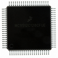
Manufacturer Part Number
MC9S12C128CFUE
Description
IC MCU 128K FLASH 25MHZ 80-QFP
Manufacturer
Freescale Semiconductor
Series
HCS12r
Specifications of MC9S12C128CFUE
Core Processor
HCS12
Core Size
16-Bit
Speed
25MHz
Connectivity
CAN, EBI/EMI, SCI, SPI
Peripherals
POR, PWM, WDT
Number Of I /o
60
Program Memory Size
128KB (128K x 8)
Program Memory Type
FLASH
Ram Size
4K x 8
Voltage - Supply (vcc/vdd)
2.35 V ~ 5.5 V
Data Converters
A/D 8x10b
Oscillator Type
Internal
Operating Temperature
-40°C ~ 85°C
Package / Case
80-QFP
Cpu Family
HCS12
Device Core Size
16b
Frequency (max)
25MHz
Interface Type
CAN/SCI/SPI
Total Internal Ram Size
4KB
# I/os (max)
60
Number Of Timers - General Purpose
8
Operating Supply Voltage (typ)
2.5/5V
Operating Supply Voltage (max)
2.75/5.5V
Operating Supply Voltage (min)
2.35/2.97V
On-chip Adc
8-chx10-bit
Instruction Set Architecture
CISC
Operating Temp Range
-40C to 85C
Operating Temperature Classification
Industrial
Mounting
Surface Mount
Pin Count
80
Package Type
PQFP
Processor Series
S12C
Core
HCS12
Data Bus Width
16 bit
Data Ram Size
4000 B
Maximum Clock Frequency
25 MHz
Number Of Programmable I/os
61
Number Of Timers
1
Operating Supply Voltage
- 0.3 V to + 6.5 V
Maximum Operating Temperature
+ 85 C
Mounting Style
SMD/SMT
3rd Party Development Tools
EWHCS12
Development Tools By Supplier
M68EVB912C32EE
Minimum Operating Temperature
- 40 C
Lead Free Status / RoHS Status
Lead free / RoHS Compliant
Eeprom Size
-
Lead Free Status / Rohs Status
Compliant
Available stocks
Company
Part Number
Manufacturer
Quantity
Price
Company:

Part Number:
MC9S12C128CFUE
Manufacturer:
ST
Quantity:
6 246
Company:
Part Number:
MC9S12C128CFUE
Manufacturer:
Freescale Semiconductor
Quantity:
10 000


Chapter 14 Serial Peripheral Interface (SPIV3) Block Description
14.4.1
The SPI operates in master mode when the MSTR bit is set. Only a master SPI module can initiate
transmissions. A transmission begins by writing to the master SPI Data Register. If the shift register is
empty, the byte immediately transfers to the shift register. The byte begins shifting out on the MOSI pin
under the control of the serial clock.
This mode fault error also sets the mode fault (MODF) flag in the SPI Status Register (SPISR). If the SPI
interrupt enable bit (SPIE) is set when the MODF flag gets set, then an SPI interrupt sequence is also
requested.
When a write to the SPI Data Register in the master occurs, there is a half SCK-cycle delay. After the delay,
SCK is started within the master. The rest of the transfer operation differs slightly, depending on the clock
format specified by the SPI clock phase bit, CPHA, in SPI Control Register 1 (see
“Transmission
424
•
•
•
S-clock
The SPR2, SPR1, and SPR0 baud rate selection bits in conjunction with the SPPR2, SPPR1, and
SPPR0 baud rate preselection bits in the SPI Baud Rate register control the baud rate generator and
determine the speed of the transmission. The SCK pin is the SPI clock output. Through the SCK
pin, the baud rate generator of the master controls the shift register of the slave peripheral.
MOSI and MISO Pins
In master mode, the function of the serial data output pin (MOSI) and the serial data input pin
(MISO) is determined by the SPC0 and BIDIROE control bits.
SS Pin
If MODFEN and SSOE bit are set, the SS pin is configured as slave select output. The SS output
becomes low during each transmission and is high when the SPI is in idle state.
If MODFEN is set and SSOE is cleared, the SS pin is configured as input for detecting mode fault
error. If the SS input becomes low this indicates a mode fault error where another master tries to
drive the MOSI and SCK lines. In this case, the SPI immediately switches to slave mode, by
clearing the MSTR bit and also disables the slave output buffer MISO (or SISO in bidirectional
mode). So the result is that all outputs are disabled and SCK, MOSI and MISO are inputs. If a
transmission is in progress when the mode fault occurs, the transmission is aborted and the SPI is
forced into idle state.
Master Mode
A change of the bits CPOL, CPHA, SSOE, LSBFE, MODFEN, SPC0,
BIDIROE with SPC0 set, SPPR2–SPPR0 and SPR2–SPR0 in master mode
will abort a transmission in progress and force the SPI into idle state. The
remote slave cannot detect this, therefore the master has to ensure that the
remote slave is set back to idle state.
Formats”).
MC9S12C-Family / MC9S12GC-Family
Rev 01.24
NOTE
Section 14.4.3,
Freescale Semiconductor
Related parts for MC9S12C128CFUE
Image
Part Number
Description
Manufacturer
Datasheet
Request
R

Part Number:
Description:
Manufacturer:
Freescale Semiconductor, Inc
Datasheet:
Part Number:
Description:
Manufacturer:
Freescale Semiconductor, Inc
Datasheet:
Part Number:
Description:
Manufacturer:
Freescale Semiconductor, Inc
Datasheet:
Part Number:
Description:
Manufacturer:
Freescale Semiconductor, Inc
Datasheet:
Part Number:
Description:
Manufacturer:
Freescale Semiconductor, Inc
Datasheet:
Part Number:
Description:
Manufacturer:
Freescale Semiconductor, Inc
Datasheet:
Part Number:
Description:
Manufacturer:
Freescale Semiconductor, Inc
Datasheet:
Part Number:
Description:
Manufacturer:
Freescale Semiconductor, Inc
Datasheet:
Part Number:
Description:
Manufacturer:
Freescale Semiconductor, Inc
Datasheet:
Part Number:
Description:
Manufacturer:
Freescale Semiconductor, Inc
Datasheet:
Part Number:
Description:
Manufacturer:
Freescale Semiconductor, Inc
Datasheet:
Part Number:
Description:
Manufacturer:
Freescale Semiconductor, Inc
Datasheet:
Part Number:
Description:
Manufacturer:
Freescale Semiconductor, Inc
Datasheet:
Part Number:
Description:
Manufacturer:
Freescale Semiconductor, Inc
Datasheet:
Part Number:
Description:
Manufacturer:
Freescale Semiconductor, Inc
Datasheet: