MC9S12C128CFUE Freescale Semiconductor, MC9S12C128CFUE Datasheet - Page 153
MC9S12C128CFUE
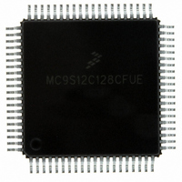
Manufacturer Part Number
MC9S12C128CFUE
Description
IC MCU 128K FLASH 25MHZ 80-QFP
Manufacturer
Freescale Semiconductor
Series
HCS12r
Specifications of MC9S12C128CFUE
Core Processor
HCS12
Core Size
16-Bit
Speed
25MHz
Connectivity
CAN, EBI/EMI, SCI, SPI
Peripherals
POR, PWM, WDT
Number Of I /o
60
Program Memory Size
128KB (128K x 8)
Program Memory Type
FLASH
Ram Size
4K x 8
Voltage - Supply (vcc/vdd)
2.35 V ~ 5.5 V
Data Converters
A/D 8x10b
Oscillator Type
Internal
Operating Temperature
-40°C ~ 85°C
Package / Case
80-QFP
Cpu Family
HCS12
Device Core Size
16b
Frequency (max)
25MHz
Interface Type
CAN/SCI/SPI
Total Internal Ram Size
4KB
# I/os (max)
60
Number Of Timers - General Purpose
8
Operating Supply Voltage (typ)
2.5/5V
Operating Supply Voltage (max)
2.75/5.5V
Operating Supply Voltage (min)
2.35/2.97V
On-chip Adc
8-chx10-bit
Instruction Set Architecture
CISC
Operating Temp Range
-40C to 85C
Operating Temperature Classification
Industrial
Mounting
Surface Mount
Pin Count
80
Package Type
PQFP
Processor Series
S12C
Core
HCS12
Data Bus Width
16 bit
Data Ram Size
4000 B
Maximum Clock Frequency
25 MHz
Number Of Programmable I/os
61
Number Of Timers
1
Operating Supply Voltage
- 0.3 V to + 6.5 V
Maximum Operating Temperature
+ 85 C
Mounting Style
SMD/SMT
3rd Party Development Tools
EWHCS12
Development Tools By Supplier
M68EVB912C32EE
Minimum Operating Temperature
- 40 C
Lead Free Status / RoHS Status
Lead free / RoHS Compliant
Eeprom Size
-
Lead Free Status / Rohs Status
Compliant
Available stocks
Company
Part Number
Manufacturer
Quantity
Price
Company:

Part Number:
MC9S12C128CFUE
Manufacturer:
ST
Quantity:
6 246
Company:
Part Number:
MC9S12C128CFUE
Manufacturer:
Freescale Semiconductor
Quantity:
10 000


4.4.3.1.2
In expanded wide modes, Ports A and B are configured as a 16-bit multiplexed address and data bus and
Port E bit 4 is configured as the E clock output signal. These signals allow external memory and peripheral
devices to be interfaced to the MCU.
Port E pins other than PE4/ECLK are configured as general purpose I/O pins (initially high-impedance
inputs with internal pull resistors enabled). Control bits PIPOE, NECLK, LSTRE, and RDWE in the
PEAR register can be used to configure Port E pins to act as bus control outputs instead of general purpose
I/O pins.
It is possible to enable the pipe status signals on Port E bits 6 and 5 by setting the PIPOE bit in PEAR, but
it would be unusual to do so in this mode. Development systems where pipe status signals are monitored
would typically use the special variation of this mode.
The Port E bit 2 pin can be reconfigured as the R/W bus control signal by writing “1” to the RDWE bit in
PEAR. If the expanded system includes external devices that can be written, such as RAM, the RDWE bit
would need to be set before any attempt to write to an external location. If there are no writable resources
in the external system, PE2 can be left as a general purpose I/O pin.
The Port E bit 3 pin can be reconfigured as the LSTRB bus control signal by writing “1” to the LSTRE bit
in PEAR. The default condition of this pin is a general purpose input because the LSTRB function is not
needed in all expanded wide applications.
The Port E bit 4 pin is initially configured as ECLK output with stretch. The E clock output function
depends upon the settings of the NECLK bit in the PEAR register, the IVIS bit in the MODE register and
the ESTR bit in the EBICTL register. The E clock is available for use in external select decode logic or as
a constant speed clock for use in the external application system.
4.4.3.1.3
This mode is used for lower cost production systems that use 8-bit wide external EPROMs or RAMs. Such
systems take extra bus cycles to access 16-bit locations but this may be preferred over the extra cost of
additional external memory devices.
Ports A and B are configured as a 16-bit address bus and Port A is multiplexed with data. Internal visibility
is not available in this mode because the internal cycles would need to be split into two 8-bit cycles.
Since the PEAR register can only be written one time in this mode, use care to set all bits to the desired
states during the single allowed write.
The PE3/LSTRB pin is always a general purpose I/O pin in normal expanded narrow mode. Although it is
possible to write the LSTRE bit in PEAR to “1” in this mode, the state of LSTRE is overridden and Port
E bit 3 cannot be reconfigured as the LSTRB output.
It is possible to enable the pipe status signals on Port E bits 6 and 5 by setting the PIPOE bit in PEAR, but
it would be unusual to do so in this mode. LSTRB would also be needed to fully understand system
activity. Development systems where pipe status signals are monitored would typically use special
expanded wide mode or occasionally special expanded narrow mode.
Freescale Semiconductor
Normal Expanded Wide Mode
Normal Expanded Narrow Mode
MC9S12C-Family / MC9S12GC-Family
Rev 01.24
Chapter 4 Multiplexed External Bus Interface (MEBIV3)
153
Related parts for MC9S12C128CFUE
Image
Part Number
Description
Manufacturer
Datasheet
Request
R

Part Number:
Description:
Manufacturer:
Freescale Semiconductor, Inc
Datasheet:
Part Number:
Description:
Manufacturer:
Freescale Semiconductor, Inc
Datasheet:
Part Number:
Description:
Manufacturer:
Freescale Semiconductor, Inc
Datasheet:
Part Number:
Description:
Manufacturer:
Freescale Semiconductor, Inc
Datasheet:
Part Number:
Description:
Manufacturer:
Freescale Semiconductor, Inc
Datasheet:
Part Number:
Description:
Manufacturer:
Freescale Semiconductor, Inc
Datasheet:
Part Number:
Description:
Manufacturer:
Freescale Semiconductor, Inc
Datasheet:
Part Number:
Description:
Manufacturer:
Freescale Semiconductor, Inc
Datasheet:
Part Number:
Description:
Manufacturer:
Freescale Semiconductor, Inc
Datasheet:
Part Number:
Description:
Manufacturer:
Freescale Semiconductor, Inc
Datasheet:
Part Number:
Description:
Manufacturer:
Freescale Semiconductor, Inc
Datasheet:
Part Number:
Description:
Manufacturer:
Freescale Semiconductor, Inc
Datasheet:
Part Number:
Description:
Manufacturer:
Freescale Semiconductor, Inc
Datasheet:
Part Number:
Description:
Manufacturer:
Freescale Semiconductor, Inc
Datasheet:
Part Number:
Description:
Manufacturer:
Freescale Semiconductor, Inc
Datasheet: