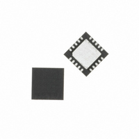
C8051T633-GM Silicon Laboratories Inc, C8051T633-GM Datasheet - Page 194

C8051T633-GM
Manufacturer Part Number
C8051T633-GM
Description
IC MCU 4KB 20PIN QFN
Manufacturer
Silicon Laboratories Inc
Series
C8051T63xr
Specifications of C8051T633-GM
Core Processor
8051
Core Size
8-Bit
Speed
25MHz
Connectivity
SMBus (2-Wire/I²C), SPI, UART/USART
Peripherals
POR, PWM, WDT
Number Of I /o
17
Program Memory Size
4KB (4K x 8)
Program Memory Type
OTP
Ram Size
768 x 8
Voltage - Supply (vcc/vdd)
1.8 V ~ 3.6 V
Oscillator Type
Internal
Operating Temperature
-40°C ~ 85°C
Package / Case
20-QFN
Processor Series
C8051T6x
Core
8051
Data Bus Width
8 bit
Data Ram Size
768 B
Interface Type
UART, SPI, SMBus
Maximum Clock Frequency
25 MHz
Number Of Programmable I/os
17
Number Of Timers
4 x 16-bit
Operating Supply Voltage
1.8 V to 3.6 V
Maximum Operating Temperature
+ 85 C
Mounting Style
SMD/SMT
3rd Party Development Tools
PK51, CA51, A51, ULINK2
Development Tools By Supplier
C8051T630DK
Minimum Operating Temperature
- 40 C
For Use With
336-1464 - KIT DEV FOR C8051T630 FAMILY
Lead Free Status / RoHS Status
Lead free / RoHS Compliant
Eeprom Size
-
Data Converters
-
Lead Free Status / Rohs Status
Details
Other names
336-1461-5
Available stocks
Company
Part Number
Manufacturer
Quantity
Price
Company:
Part Number:
C8051T633-GM
Manufacturer:
Silicon
Quantity:
270
C8051T630/1/2/3/4/5
25.3. Capture/Compare Modules
Each module can be configured to operate independently in one of six operation modes: edge-triggered
capture, software timer, high-speed output, frequency output, 8 to 11-bit pulse width modulator, or 16-bit
pulse width modulator. Each module has Special Function Registers (SFRs) associated with it in the CIP-
51 system controller. These registers are used to exchange data with a module and configure the module's
mode of operation. Table 25.2 summarizes the bit settings in the PCA0CPMn and PCA0PWM registers
used to select the PCA capture/compare module’s operating mode. Note that all modules set to use 8, 9,
10, or 11-bit PWM mode must use the same cycle length (8–11 bits). Setting the ECCFn bit in a
PCA0CPMn register enables the module's CCFn interrupt.
194
Operational Mode
Capture triggered by positive edge on CEXn
Capture triggered by negative edge on CEXn
Capture triggered by any transition on CEXn
Software Timer
High Speed Output
Frequency Output
8-Bit Pulse Width Modulator (Note 7)
9-Bit Pulse Width Modulator (Note 7)
10-Bit Pulse Width Modulator (Note 7)
11-Bit Pulse Width Modulator (Note 7)
16-Bit Pulse Width Modulator
Notes:
Table 25.2. PCA0CPM and PCA0PWM Bit Settings for PCA Capture/Compare
1. X = Don’t Care (no functional difference for individual module if 1 or 0).
2. A = Enable interrupts for this module (PCA interrupt triggered on CCFn set to 1).
3. B = Enable 8th, 9th, 10th or 11th bit overflow interrupt (Depends on setting of CLSEL[1:0]).
4. C = When set to 0, the digital comparator is off. For high speed and frequency output modes, the
5. D = Selects whether the Capture/Compare register (0) or the Auto-Reload register (1) for the associated
6. E = When set, a match event will cause the CCFn flag for the associated channel to be set.
7. All modules set to 8, 9, 10 or 11-bit PWM mode use the same cycle length setting.
associated pin will not toggle. In any of the PWM modes, this generates a 0% duty cycle (output = 0).
channel is accessed via addresses PCA0CPHn and PCA0CPLn.
Bit Number 7 6 5 4 3 2 1 0 7 6 5
Modules
Rev. 1.0
X X 1 0 0 0 0 A 0 X B XXX
X X 0 1 0 0 0 A 0 X B XXX
X X 1 1 0 0 0 A 0 X B XXX
X C 0 0 1 0 0 A 0 X B XXX
X C 0 0 1 1 0 A 0 X B XXX
X C 0 0 0 1 1 A 0 X B XXX
0 C 0 0 E 0 1 A 0 X B XXX
0 C 0 0 E 0 1 A D X B XXX
0 C 0 0 E 0 1 A D X B XXX
0 C 0 0 E 0 1 A D X B XXX
1 C 0 0 E 0 1 A 0 X B XXX
PCA0CPMn
PCA0PWM
4–2
1–0
XX
XX
XX
XX
XX
XX
XX
00
01
10
11


