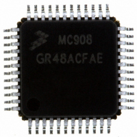
MC908GR48ACFAE Freescale Semiconductor, MC908GR48ACFAE Datasheet - Page 219

MC908GR48ACFAE
Manufacturer Part Number
MC908GR48ACFAE
Description
IC MCU 48K FLASH 8MHZ 48-LQFP
Manufacturer
Freescale Semiconductor
Series
HC08r
Datasheet
1.MC908GR32ACFJE.pdf
(314 pages)
Specifications of MC908GR48ACFAE
Core Processor
HC08
Core Size
8-Bit
Speed
8MHz
Connectivity
SCI, SPI
Peripherals
LVD, POR, PWM
Number Of I /o
37
Program Memory Size
48KB (48K x 8)
Program Memory Type
FLASH
Ram Size
1.5K x 8
Voltage - Supply (vcc/vdd)
3 V ~ 5.5 V
Data Converters
A/D 24x10b
Oscillator Type
Internal
Operating Temperature
-40°C ~ 85°C
Package / Case
48-LQFP
Processor Series
HC08GR
Core
HC08
Data Bus Width
8 bit
Data Ram Size
1.5 KB
Interface Type
ESCI/SPI
Maximum Clock Frequency
8 MHz
Number Of Programmable I/os
53
Number Of Timers
8
Maximum Operating Temperature
+ 85 C
Mounting Style
SMD/SMT
Development Tools By Supplier
FSICEBASE, DEMO908GZ60E, M68CBL05CE, M68EML08GPGTE
Minimum Operating Temperature
- 40 C
On-chip Adc
24-ch x 10-bit
Controller Family/series
HC08
No. Of I/o's
37
Ram Memory Size
1.5KB
Cpu Speed
8MHz
No. Of Timers
2
Embedded Interface Type
SCI, SPI
Rohs Compliant
Yes
Lead Free Status / RoHS Status
Lead free / RoHS Compliant
Eeprom Size
-
Lead Free Status / Rohs Status
Lead free / RoHS Compliant
Available stocks
Company
Part Number
Manufacturer
Quantity
Price
Company:
Part Number:
MC908GR48ACFAE
Manufacturer:
Freescale Semiconductor
Quantity:
10 000
- Current page: 219 of 314
- Download datasheet (5Mb)
SPRF — SPI Receiver Full Bit
ERRIE — Error Interrupt Enable Bit
OVRF — Overflow Bit
MODF — Mode Fault Bit
SPTE — SPI Transmitter Empty Bit
MODFEN — Mode Fault Enable Bit
Freescale Semiconductor
This clearable, read-only flag is set each time a byte transfers from the shift register to the receive data
register. SPRF generates a CPU interrupt request if the SPRIE bit in the SPI control register is set also.
During an SPRF CPU interrupt, the CPU clears SPRF by reading the SPI status and control register
with SPRF set and then reading the SPI data register.
Reset clears the SPRF bit.
This read/write bit enables the MODF and OVRF bits to generate CPU interrupt requests. Reset clears
the ERRIE bit.
This clearable, read-only flag is set if software does not read the byte in the receive data register before
the next full byte enters the shift register. In an overflow condition, the byte already in the receive data
register is unaffected, and the byte that shifted in last is lost. Clear the OVRF bit by reading the SPI
status and control register with OVRF set and then reading the receive data register. Reset clears the
OVRF bit.
This clearable, read-only flag is set in a slave SPI if the SS pin goes high during a transmission with
MODFEN set. In a master SPI, the MODF flag is set if the SS pin goes low at any time with the
MODFEN bit set. Clear MODF by reading the SPI status and control register (SPSCR) with MODF set
and then writing to the SPI control register (SPCR). Reset clears the MODF bit.
This clearable, read-only flag is set each time the transmit data register transfers a byte into the shift
register. SPTE generates an SPTE CPU interrupt request if SPTIE in the SPI control register is set
also.
During an SPTE CPU interrupt, the CPU clears SPTE by writing to the transmit data register.
Reset sets the SPTE bit.
This read/write bit, when set, allows the MODF flag to be set. If the MODF flag is set, clearing MODFEN
does not clear the MODF flag. If the SPI is enabled as a master and the MODFEN bit is 0, then the SS
pin is available as a general-purpose I/O.
If the MODFEN bit is 1, then the SS pin is not available as a general-purpose I/O. When the SPI is
enabled as a slave, the SS pin is not available as a general-purpose I/O regardless of the value of
MODFEN. See
1 = Receive data register full
0 = Receive data register not full
1 = MODF and OVRF can generate CPU interrupt requests
0 = MODF and OVRF cannot generate CPU interrupt requests
1 = Overflow
0 = No overflow
1 = SS pin at inappropriate logic level
0 = SS pin at appropriate logic level
1 = Transmit data register empty
0 = Transmit data register not empty
Do not write to the SPI data register unless SPTE is high.
MC68HC908GR60A • MC68HC908GR48A • MC68HC908GR32A Data Sheet, Rev. 5
15.11.4 SS (Slave Select).
NOTE
I/O Registers
219
Related parts for MC908GR48ACFAE
Image
Part Number
Description
Manufacturer
Datasheet
Request
R
Part Number:
Description:
Manufacturer:
Freescale Semiconductor, Inc
Datasheet:
Part Number:
Description:
Manufacturer:
Freescale Semiconductor, Inc
Datasheet:
Part Number:
Description:
Manufacturer:
Freescale Semiconductor, Inc
Datasheet:
Part Number:
Description:
Manufacturer:
Freescale Semiconductor, Inc
Datasheet:
Part Number:
Description:
Manufacturer:
Freescale Semiconductor, Inc
Datasheet:
Part Number:
Description:
Manufacturer:
Freescale Semiconductor, Inc
Datasheet:
Part Number:
Description:
Manufacturer:
Freescale Semiconductor, Inc
Datasheet:
Part Number:
Description:
Manufacturer:
Freescale Semiconductor, Inc
Datasheet:
Part Number:
Description:
Manufacturer:
Freescale Semiconductor, Inc
Datasheet:
Part Number:
Description:
Manufacturer:
Freescale Semiconductor, Inc
Datasheet:
Part Number:
Description:
Manufacturer:
Freescale Semiconductor, Inc
Datasheet:
Part Number:
Description:
Manufacturer:
Freescale Semiconductor, Inc
Datasheet:
Part Number:
Description:
Manufacturer:
Freescale Semiconductor, Inc
Datasheet:
Part Number:
Description:
Manufacturer:
Freescale Semiconductor, Inc
Datasheet:
Part Number:
Description:
Manufacturer:
Freescale Semiconductor, Inc
Datasheet:


