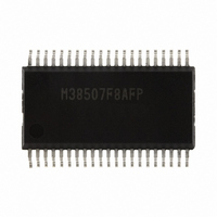
M38507F8AFP#U1 Renesas Electronics America, M38507F8AFP#U1 Datasheet - Page 13

M38507F8AFP#U1
Manufacturer Part Number
M38507F8AFP#U1
Description
IC 740/3850 MCU FLASH 42SSOP
Manufacturer
Renesas Electronics America
Series
740/38000r
Datasheet
1.M38507F8AFPU1.pdf
(61 pages)
Specifications of M38507F8AFP#U1
Core Processor
740
Core Size
8-Bit
Speed
12.5MHz
Connectivity
SIO, UART/USART
Peripherals
PWM, WDT
Number Of I /o
32
Program Memory Size
32KB (32K x 8)
Program Memory Type
FLASH
Ram Size
1K x 8
Voltage - Supply (vcc/vdd)
1.8 V ~ 5.5 V
Data Converters
A/D 9x10b
Oscillator Type
Internal
Operating Temperature
-20°C ~ 85°C
Package / Case
42-SSOP
Package
42SSOP
Family Name
740
Maximum Speed
12.5 MHz
Operating Supply Voltage
5 V
Data Bus Width
8 Bit
Number Of Programmable I/os
34
Interface Type
UART
On-chip Adc
9-chx10-bit
Number Of Timers
4
Lead Free Status / RoHS Status
Lead free / RoHS Compliant
Eeprom Size
-
Available stocks
Company
Part Number
Manufacturer
Quantity
Price
3850 Group (Spec.A QzROM version)
Rev.2.13
REJ03B0125-0213
MEMORY
• Special Function Register (SFR) Area
The Special Function Register area in the zero page contains
control registers such as I/O ports and timers.
• RAM
RAM is used for data storage and for stack area of subroutine
calls and interrupts.
• ROM
The first 128 bytes and the last 2 bytes of ROM are reserved for
device testing and the rest is user area for storing programs.
In the QzROM version, 1 byte of address FFDB
reserved area.
• Interrupt Vector Area
The interrupt vector area contains reset and interrupt vectors.
• Zero Page
Access to this area with only 2 bytes is possible in the zero page
addressing mode.
• Special Page
Access to this area with only 2 bytes is possible in the special
page addressing mode.
Fig 8.
Memory map diagram
RAM area
ROM area
ROM size
RAM size
12288
16384
20480
24576
28672
32768
36864
40960
45056
49152
53248
57344
61440
Apr 17, 2009
1024
1536
2048
4096
8192
(bytes)
(bytes)
192
256
384
512
640
768
896
Address
Address
XXXX
YYYY
01BF
02BF
03BF
D000
C000
00FF
013F
023F
033F
043F
063F
083F
F000
E000
B000
A000
9000
8000
7000
6000
5000
4000
3000
2000
1000
Page 11 of 56
16
16
16
16
16
16
16
16
16
16
16
16
16
16
16
16
16
16
16
16
16
16
16
16
16
16
16
Address
ZZZZ
F080
E080
D080
C080
B080
A080
9080
8080
7080
6080
5080
4080
3080
2080
1080
16
16
16
16
16
16
16
16
16
16
16
16
16
16
16
16
16
is also a
RAM
ROM
• ROM Code Protect Address (address FFDB
Address FFDB
the ROM code protect address. “00
when selecting the protect bit write by using a serial programmer
or selecting protect enabled for writing shipment by Renesas
Technology corp.. When “00
address, the protect function is enabled, so that reading or writing
from/to QzROM is disabled by a serial programmer.
As for the QzROM product in blank, the ROM code is protected
by selecting the protect bit write at ROM writing with a serial
programmer.
As for the QzROM product shipped after writing, “00
enabled) or “FF
code protect address when Renesas Technology corp. performs
writing.
The writing of “00
setup (“MASK option” written in the mask file converter) when
ordering.
<Notes>
Since the contents of RAM are undefined at reset, be sure to set
an initial value before use.
XXXX
YYYY
FFDC
FFDB
FFFE
ZZZZ
FFFF
FF00
0000
0040
0100
16
16
16
16
16
16
16
16
16
16
16
(ROM code protect address)
16
Reserved ROM area
Reserved ROM area
Interrupt vector area
16
User ROM area
Reserved ROM area
, which is the reserved ROM area of QzROM, is
” (protect disabled) is written into the ROM
16
(128 bytes)
” or “FF
SFR area
Not used
16
16
” can be selected as ROM option
” is set to the ROM code protect
16
” is written into this address
Special page
Zero page
16
16
)
” (protect


